


Smart building technology is expanding rapidly. The market for these systems will grow from USD 171.44 billion in 2026 to USD 821.60 billion by 2033, a 25.1% compound annual growth rate. Yet a core problem persists: the electronics inside building controllers, energy monitors, and low-power sensors can consume significant power when poorly designed. Buildings already account for 40% of global energy consumption, and 30% of that energy goes to waste.
How can you design and manufacture the printed circuit board (PCB) at the heart of these devices to minimize energy consumption without sacrificing performance or reliability? This guide answers that question. You will learn practical strategies for low power PCBA assembly, from component selection to circuit layout and manufacturing processes. The choices you make at the PCB level determine whether your building infrastructure truly saves energy or quietly wastes it. Energy-efficient design starts here—on the circuit board itself.
Key Takeaways
Choose DC-DC converters over LDOs for large voltage drops to save up to 6W per board.
Use deep-sleep modes and intelligent sampling to cut standby power to microamps.
Optimize PCB layout with short traces, ground planes, and thermal vias to reduce energy loss.
Adopt energy-efficient manufacturing like modern reflow ovens and lead-free solder to cut waste.
Test assembled boards with current profiling and thermal imaging to ensure efficiency.
Low Power PCBA Assembly for Smart Building Devices
The printed circuit board at the center of your building controller determines the device’s overall efficiency. The choices of components on the PCB affect system performance. The circuit must also consider signal distribution across the board. Market demand for greener structures drives engineers to minimize waste. A strategic low power PCBA assembly approach starts with the PCB itself. The board becomes the foundation for efficient building infrastructure. This foundation determines whether your device saves energy or wastes it.
Identifying Primary Sources of Power Consumption
Three main areas drain current in a typical smart building device: standby leakage, active processing draw, and conversion losses. Standby leakage occurs when components on the PCB draw current even in idle states. A poorly designed heat pump control board illustrates the conversion problem. When the power distribution stage on the PCB uses an inefficient regulator, the board wastes current as heat. This waste adds up across many boards in a single building, increasing operational costs.
Deep-sleep modes offer a solution for standby losses. By deactivating the CPU and keeping only essential modules active, the circuit on the PCB can reduce draw to a few nanoamps. In deep-sleep mode, consumption drops to a few microamps, enabling battery-powered devices to last months or years. Intelligent sampling strategies also cut sensor draw by 90% or more while maintaining data quality. Circuit layout directly influences how well these modes perform.
Balancing Performance with Energy Efficiency Goals
You face a common engineering challenge. Your device must process real-time data from sensors, run control algorithms, and communicate with building systems. Control systems require reliable operation under varying loads. Yet every computation cycle on the PCB consumes current. The balance between performance and efficiency matters for both battery-powered sensors and mains-powered controllers.
Dynamic Voltage and Frequency Scaling (DVFS) addresses this trade-off. DVFS adjusts processor performance on the PCB based on workload demands, reducing draw during low-activity periods. The relationship between voltage changes and draw follows a cubic pattern, so small voltage reductions yield significant savings. This approach keeps your building infrastructure responsive while minimizing waste. The design choices you make at the printed circuit board level directly impact whether your device meets its efficiency targets. A focus on low power pcba assembly ensures your product delivers real savings. The assembly process requires careful quality checks.
Design Strategies for Energy-Efficient PCBs
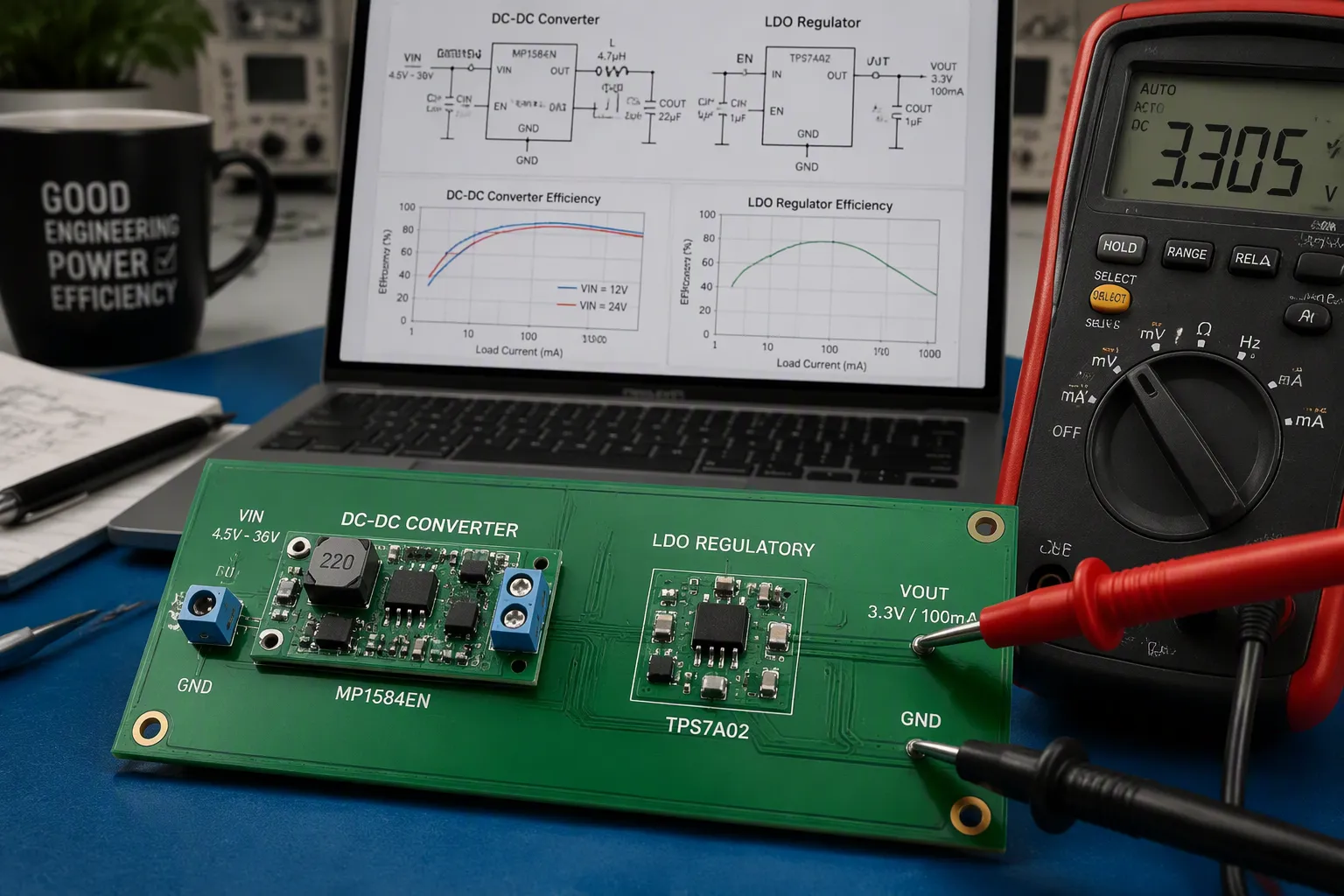
Your component choices on the pcb determine the efficiency ceiling for your entire device. Two regulation approaches dominate: linear regulators (LDOs) and switching regulators (DC-DC converters). The gap between them is substantial.
Conversion Scenario | LDO Efficiency | DC-DC Converter Efficiency |
|---|---|---|
12V to 3.3V | 27.5% | 85-95% |
5V to 3.3V @ 100mA | 66% | Not specified |
For a 12V to 3.3V step-down at 1A, an SMPS can save up to 6W compared to a linear regulator. LDOs suit low-current applications with small voltage differentials, where dissipation stays minimal. DC-DC converters achieve dramatically higher efficiency for large voltage drops. A switching regulator wastes only ~0.3W for the same conversion, reducing thermal stress and extending battery life in portable devices.
Microcontroller selection matters equally. Choose a chip with low-power sleep modes that deactivate the CPU while keeping essential modules active. For wireless communication, match the protocol to your use case. LoRaWAN delivers very low power for long-range, infrequent transmissions. Bluetooth LE works best for short-range applications. NB-IoT suits urban sensors with cellular connectivity. WiFi consumes high power; use it only with deep sleep and short bursts.
Selecting Components for Low Power and High Reliability
Every component on your printed circuit board contributes to the total draw. The efficiency formula for an LDO is straightforward: Efficiency = (Vout / Vin) × 100%. A 5V to 3.3V conversion yields only 66% efficiency. At 1A load, the LDO dissipates 1.7W as heat, requiring heat sinks or larger PCB areas for thermal management. These losses accumulate across many boards in a building, increasing operational costs.
Your component selection must balance efficiency with reliability. Choose ceramic capacitors with X7R or C0G types for their stability and low ESR. Select regulators rated for your full input range. Verify that every part operates within its safe thermal envelope across the expected ambient temperatures. These choices affect the lifespan of your pcb and the overall device reliability.
Optimizing Circuit Layout and Power Management
A well-designed layout reduces power loss and improves thermal management. Shorten trace lengths to minimize resistance. Reducing trace resistance from 0.1Ω to 0.05Ω on a 1A line halves power loss from 0.1W to 0.05W. Use a continuous, un-split ground plane to provide a low-impedance return path, reducing noise and managing EMI.
Strategy | Mechanism & Quantitative Benefit |
|---|---|
Shorten trace lengths | Reducing trace resistance from 0.1Ω to 0.05Ω on a 1A line halves power loss from 0.1W to 0.05W. |
Optimize ground planes | A continuous ground plane provides a low-impedance return path, reducing noise and power loss. |
Use thermal vias | Placing 10-15 thermal vias under a power IC can reduce its operating temperature by 10-15°C. |
Place decoupling capacitors | A 0.1μF capacitor near an MCU stabilizes voltage and reduces ripple. |
Decoupling capacitor placement follows clear rules. Place capacitors close to IC power pins, within 1-2mm when possible. Use short, wide traces to keep loop inductance low. Combine capacitor values to cover different frequency ranges: a 0.1µF capacitor paired with a 1µF capacitor handles both high-frequency noise and lower fluctuations. Allocate one capacitor per power pin. Minimize the loop area formed by the power pin, capacitor, and ground to reduce electromagnetic interference.
Thermal vias deserve attention. Placing 10-15 thermal vias under a power IC can reduce its operating temperature by 10-15°C, improving efficiency and preventing thermal runaway. This practice directly impacts the lifespan of your pcb and the reliability of your building systems. A cooler circuit operates more efficiently and lasts longer.
Your layout also affects power distribution across the board. Route power and ground with wide, short traces to reduce resistance and inductance. Maintain symmetry to prevent uneven current distribution. Prioritize direct, unbroken paths from capacitors to ICs to enhance stability. These design choices determine whether your electronics deliver the efficiency your building infrastructure promises. The circuit layout you create today shapes the energy performance of your systems for years to come.
Manufacturing Processes for Sustainable PCB Assembly
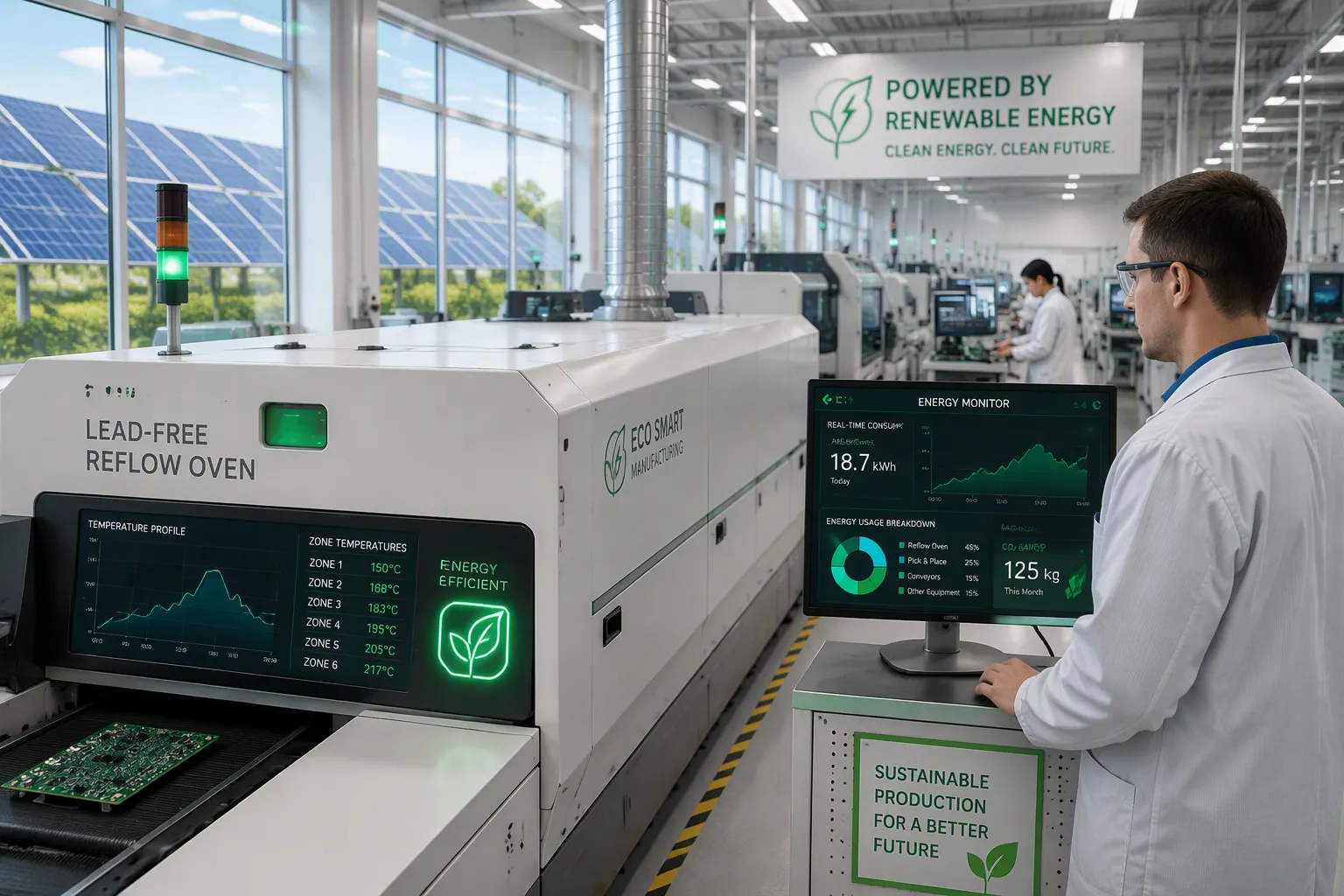
Your design choices set the efficiency target. The assembly process determines whether you hit it. Each printed circuit board must be built with care. The production line can waste resources if you do not optimize it. Eco-friendly manufacturing practices reduce this waste.
Reducing Energy and Waste in the Assembly Line
Upgrade to modern reflow ovens with precise temperature control. These ovens use less energy than older models. Energy-efficient reflow ovens with zoned heating achieve power reduction. Keep your ovens in optimal condition. Poor maintenance causes efficiency loss. These savings benefit every pcb you produce.
Practice | Specific Action | Savings Claim |
|---|---|---|
Equipment Upgrade | Modern reflow ovens with precise temperature control | Less energy |
SMT Assembly | Energy-efficient reflow ovens with zoned heating | Power reduction |
Maintenance | Keep reflow ovens in optimal condition | Avoid efficiency loss |
Design Optimization | Minimize layer count and optimize component placement | Reduces material and electricity for etching/laminating |
Etching Process | Use laser etching instead of wet etching | Consumes less electricity and produces less chemical waste |
Lean manufacturing eliminates unnecessary steps. Shift your facility to solar or wind generation. Replace traditional UV lamps with LED-based curing equipment. LED equipment consumes significantly less electricity. Energy-efficient ovens and reflow soldering machines lower consumption during the pcb production process.
Material choices matter for sustainability. Use lead-free solder. Low-temperature soldering techniques consume less electricity during the pcb production process. Consider recyclable substrates like Soluboard. These break down at end of life. Minimize layer count and optimize component placement on your pcb. This reduces material and electricity for etching and laminating. Use laser etching instead of wet etching. Laser etching consumes less electricity and produces less chemical waste.
Your pcb production process should also consider power distribution across the board. Efficient power distribution starts with good design. Solder joint quality affects the resistance of power distribution paths. Poor joints add resistance and waste electricity. Your production partner must control soldering parameters tightly.
Testing and Validation for Energy Performance
Verifying performance during production is essential for reliable pcb assembly. Your assembled pcb must meet its low-power design specifications. Each printed circuit board undergoes current consumption profiling. This test measures the actual draw of the circuit under operating conditions. The circuit must operate within its efficiency targets. The circuit design affects system performance. The circuit temperature influences leakage current. Current consumption profiling catches excessive leakage or inefficient power conversion.
Thermal imaging identifies hot spots on your pcb. A hot component indicates electricity waste as heat. Thermal imaging reveals poor solder joints, inadequate thermal vias, or components that exceed their rated limits. Fix these issues before the pcb enters service.
These tests are crucial for applications like solar inverters and battery management systems for smart grids. A solar inverter pcb wastes electricity as heat. A battery management system pcb drains batteries faster. Testing ensures your pcb performs as designed.
Validation also includes verifying that your low power pcba assembly meets specifications. Your low power pcba assembly approach should be validated through functional tests. Document test results for each pcb. Use this data to improve your design and production process. Your pcb testing protocol should include tests at multiple operating points. Measure current draw at idle, active, and sleep modes. Compare results to your design targets.
A thorough validation program catches problems early. Early detection saves costs. Your assembly partner should have documented test procedures. Ask for evidence of their testing capabilities. This step ensures your pcb delivers the efficiency your building systems require.
Applications and Future Trends in Green Technology
Enabling Smart Building Certifications and Renewable Energy Systems
Your energy-efficient pcb design directly contributes to achieving green building certifications like LEED and BREEAM. These standards evaluate the energy performance of your building infrastructure. A well-designed pcb reduces the power consumption of controllers, sensors, and monitors. This reduction helps your building earn points toward certification. Your building systems operate more efficiently with an optimized pcb. Power distribution across the pcb affects overall efficiency. Custom pcbs for smart home devices demonstrate this principle. A thermostat pcb with efficient power management draws less current. A lighting control pcb with optimized layout wastes less energy as heat. Rugged pcb assemblies for smart city applications deploy these same principles outdoors. Street lighting controllers, air quality monitors, and traffic management systems all benefit from efficient pcb design. Your building infrastructure becomes more sustainable when the pcbs inside it operate efficiently.
Real-world projects validate this approach. A university team demonstrated a solar harvesting system for low-power pcb applications. The system used an organic photovoltaic cell assembled on a pcb with a regulatory IC. Testing showed strong performance when the photovoltaic faced south. North-facing orientation still offered feasible charging for low-drain uses. This confirms the practical value of harvesting-based designs for future products. Your pcb can integrate this technology to reduce reliance on batteries.
Innovations in Low-Power Electronics and Materials
Emerging trends push the boundaries of what your circuit can achieve. Energy harvesting technology continues to advance. The SELECT project develops a scalable platform for batteryless electronics. It starts with electronic shelf labels powered by indoor ambient light. Key integrated technologies include ultra-low-power microcontrollers from ONiO, photovoltaics from Epishine, eco-friendly supercapacitors from Ligna Energy, and fully recyclable pcb laminates from Jiva Materials. This collaboration aims to eliminate traditional batteries and reduce electronic waste. Your electronics can benefit from these innovations.
Another harvesting application shows measurable results. A system generates power at speed, with a compact PCB area for power management. The pcb thickness stays within a few millimeters. This system successfully powered a commercial Bluetooth tyre pressure sensor. Your circuit can achieve similar results for building sensors.
Sustainable pcb materials also evolve rapidly. The Jiva Soluboard represents a fully recyclable pcb substrate. It demonstrates a carbon footprint reduction compared to conventional materials. Other options include halogen-free laminates and recyclable substrates. Biodegradable pcb materials use banana fibre and wheat gluten to develop organic circuit boards that naturally decompose. Graphene and nanotechnology offer high electrical conductivity while being more environmentally friendly than traditional copper-based pcbs. Your flexible printed circuit boards can incorporate these materials to reduce environmental impact.
These innovations connect to the core goal of reducing the carbon footprint of electronic devices throughout their entire lifecycle. Your sustainable energy systems benefit from efficient power distribution across the board. Your building infrastructure operates more efficiently. Your electronic devices last longer and waste less. The technology choices you make today determine the environmental impact of your products.
Energy efficiency spans design, manufacturing, and validation. You cannot treat these stages separately. Your pcb choices determine whether your building infrastructure truly saves power. Every circuit decision matters. Your pcb layout affects thermal performance. Your pcb component selection drives conversion losses. Your pcb testing validates real-world draw.
These strategies are not optional extras. They form the foundation of responsible engineering. Your building systems depend on efficient pcb assembly. Your energy goals require it. Your building infrastructure performs better with each improvement.
Adopting these practices gives you a competitive edge. You build more reliable products. Your devices last longer. Your customers save money.
Start now. Integrate these principles into your next project. Begin at the initial design review. Your pcb will deliver the efficiency your building deserves.
FAQ
How does PCB layout affect standby power consumption?
Your PCB layout directly controls leakage paths and parasitic resistance. Short, wide traces minimize resistive losses. A continuous ground plane reduces noise that forces components to draw extra current. Proper decoupling capacitor placement stabilizes voltage, preventing inefficient power distribution across the board.
When should I choose a DC-DC converter over an LDO?
Choose a DC-DC converter when your voltage drop exceeds 2V or your current draw exceeds 100mA. A 12V-to-3.3V conversion with an LDO yields only 27.5% efficiency. A switching regulator achieves 85-95% efficiency. Use LDOs only for small differentials and low currents.
What testing methods verify energy performance during assembly?
Current consumption profiling measures actual draw during idle, active, and sleep modes. Thermal imaging reveals hot spots that indicate wasted energy. These tests ensure your assembled PCB meets its low-power specifications before deployment in building systems.
How do material choices impact sustainability?
Lead-free solder and low-temperature techniques reduce energy during assembly. Recyclable substrates like Soluboard cut carbon footprint. Your circuit design choices affect the entire lifecycle of the device. Every PCB you produce contributes to the overall efficiency of your building infrastructure.
See Also
Intelligent Building Circuit Boards For Malaysian IoT Firms
Bespoke Edge AI Boards For American Hardware New Ventures
AI IoT Circuit Board Production For Malaysian Hardware Businesses
Tailored AI Board Fabrication For Mexican Electronics Enterprises