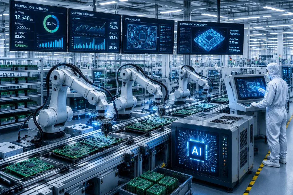
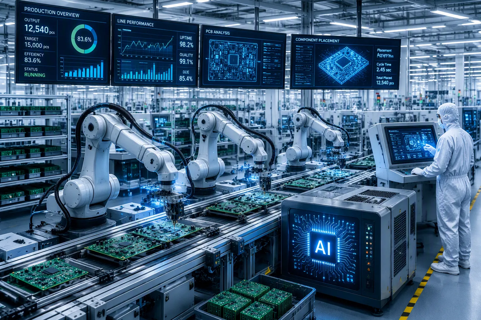
You might ask if an AI PCBA factory in China truly gives you value or just follows a trend. The proof is real. These plants fix ongoing issues: uneven quality, slow delivery, and pricey testing. They use artificial intelligence to check every solder point, improve part placement, and adjust steps as they work. This method brings better accuracy and quicker results than older factories. You get steady, expected results for your PCB projects. An ai pcba partner cuts down on mistakes and offers data-based checks you can rely on. This guide looks at their skills, costs, and how to pick one, so you can choose wisely for your next job.
Key Takeaways
AI factories in China use smart machines to inspect every component. This leads to fewer errors and higher quality for your circuit boards.
AI inspection saves money over time. It cuts down on waste and rework, so your project gets more value.
Pick a factory that has the right certifications and experience. This makes sure they meet your industry’s standards.
Talking clearly and having a full-service partner can help you avoid delays. They take care of design, assembly, and testing for you.
AI technology and a strong partnership help make reliable products. Your devices will work well and arrive on time.
AI PCBA Capabilities in China
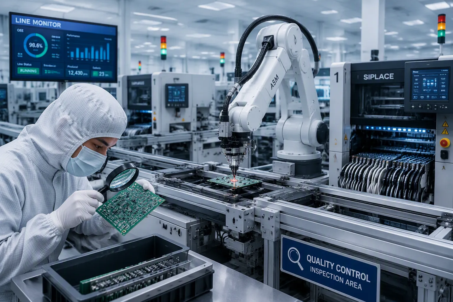
China is a top place for ai pcba manufacturing. Many factories provide full services like board design, fabrication, assembly, SMT, and turnkey. Many leading factories have extensive experience in medical, automotive, AI robotics, and industrial automation. This background with ai helps them keep improving their methods. If you need a partner for ai devices, China offers this know-how.
Design, Prototyping, and Turnkey Services
A full turnkey service handles everything from design to delivery. You share your idea. The factory does the rest. This covers board layout, part sourcing, prototyping, assembly, and testing. For hdi technology projects, this method saves time. The factory uses ai to improve part placement. Many designs need an ai hdi pcb structure for tight part packing.
A key part of this process is the DFM review. The factory checks your design before making it. The table below shows how PCB DFM review works with DFA review.
Aspect | PCB DFM Review | PCBA DFA Review |
|---|---|---|
Performed by | PCB manufacturer | PCB assembly house |
Purpose | Check design can be made to spec | Check boards can be assembled to spec; checks component footprints |
Files used | Gerber, ODB++, IPC-2581 | PCB production data, component data, assembly documentation |
Method | Engineer checklist with automated tools | Engineer checklist plus manual footprint/datasheet review |
Time | Minutes | Time-consuming, labor-intensive |
In ai pcba turnkey services, DFM review is the first key step. It uses Gerber files to find defects before production. This leads to part sourcing and incoming checks. This ensures your high-quality hdi pcba manufacturing project starts on a strong base.
For projects needing one-stop ai hdi pcb manufacturing, this combined workflow cuts redesigns and delays. Factories that mix hdi skills with automated inspection give better results.
Advanced Assembly and Inspection Technologies
For ai server pcbs, the factory uses advanced SMT assembly lines:
5+ SMT production lines
20M+ component placements per day
500K+ THT placements per day
Dedicated assembly cells for customer-specific requirements
The factory handles both prototypes and volume production without changing suppliers.
The SMT assembly process for ai server pcbs includes these checkpoints:
Solder Paste Inspection (SPI) using PARMI SPI HS60L. This checks solder paste volume, printing consistency, and position accuracy before part placement.
Automated Optical Inspection (AOI) using ZHENHUA XING systems or VCTA-A410. This finds missing parts, wrong placement, incorrect polarity, and visible soldering issues after placement.
X-Ray Inspection using AX7900. This checks hidden solder joints and internal connections in BGA, QFN, and other high-density semiconductor packages.
For ai devices, controlled thermal process management is vital. The factory uses SUNEAST SER-708AH and SER-710A equipment. These keep a steady temperature profile during reflow soldering. This ensures stable solder quality and boosts long-term reliability.
Beyond the physical assembly process, the factory offers supply chain management through BOM procurement services. This includes BOM review, part sourcing, and supplier coordination. It keeps your ai-driven devices production schedules on track.
This full set of capabilities makes the china pcb market a strong choice. Whether you need a high-density-interconnected printed circuit board for ai applications or a standard board, these factories use ai to deliver steady results. The mix of hdi design support and automated inspection gives you confidence in every batch.
Ensuring Quality Control and Reliability
Quality control determines how well your ai pcba project performs. Chinese factories now lead the way with automated inspection systems, reflecting the industry’s focus on steady, reliable quality checks.
The Role of AI-Driven Inspection
Old rule-based AOI systems often flag too many false positives. These false alarms waste time and lead to needless rework. AI changes that. Trained on millions of verified board images, these systems cut false-call rates to under 0.5%. The system learns to separate normal reflections from real defect signs. This matters for shiny surfaces common on LED boards. Manual checks often get these surfaces wrong. The automated system handles them without mistakes.
For complex boards like an ai hdi pcb, hidden defects inside dense layers are tricky. X-ray inspection with image analysis catches these problems. The system checks every solder joint under BGA packages. You get the same reliable results on every board in your batch. This deep inspection supports the dependability that ai devices need.
Building Trust in Automated Manufacturing
You might wonder if automated inspection can match human judgment. The data shows it beats humans at finding defects consistently. Every pcb goes through the same strict inspection process. The system never gets tired. Each board gets the same thorough check. This consistency builds trust in the manufacturing process.
Factories making ai server pcbs need this reliability. One defect can cause system failure. The stakes are high for high-performance computing. The same holds for ai applications where performance depends on perfect assembly.
For high-density designs, hdi technology demands precise quality control. The narrow traces leave no room for error. Another hdi advantage is packing more connections into less space. This hdi feature requires automated inspection to verify every link. Whether you need a simple pcb or a complex multilayer board, these factories deliver consistent quality. The mix of automated checks gives you confidence in every shipment.
Cost Analysis: AI vs. Traditional PCBA
You might think an AI-driven factory costs more at first. The starting price can be higher. But the long-term view is different. AI systems lower defects, cut rework, and speed up delivery. These savings build fast. For many projects, the total cost with an AI PCBA partner in China ends up less than with a traditional plant.
Comparing Upfront and Operational Costs
Traditional factories use manual checks and older machines. Their setup costs look lower at first. But you pay for that gap during production. Human inspectors miss flaws. They also reject good boards by mistake. Both issues cost you money.
AI inspection changes this balance. In one PCB LED defect detection case, the overkill rate fell from 1.3% to 0.45%. The escape rate dropped from 0.93% to 0.07%. Overkill means good boards thrown away. Escape means bad boards sent to customers. Both shrink a lot with AI.
The savings go beyond inspection. AI systems also cut false alarms by up to 15%. They spot defects with an error rate of 2% or less. This accuracy means less wasted material and fewer rework cycles. Your production line runs smoother. You order fewer replacement parts. You spend less on scrap disposal.
Long-Term ROI and Risk Mitigation
The return on investment for AI inspection is strong. AI vision systems cut defect costs by 80-95% in high-speed manufacturing. Think of a plant making 1,200 parts per day. That operation saves $342,000 in yearly labor costs. The platform fee is $78,000. The starting investment is $240,000. The payback period lands within 8 months. The three-year ROI reaches 374%.
These numbers matter for your project planning. A traditional factory might quote a lower unit price. But hidden costs show up later. Rework expenses pile up. Customer returns hurt your reputation. Delays push your product launch back. Each problem cuts into your profit margin.
Full-turnkey services lower these risks further. The factory handles component sourcing and DFM review before production starts. This catches design issues early. You avoid costly redesigns. The smooth process moves you from prototype to mass production faster. For complex boards like an ai hdi pcb, this efficiency proves vital. The hdi technology demands precision. AI inspection checks every connection. You get reliable results without constant oversight.
The cost advantage becomes clear when you add up total project expenses. An AI factory in China offers fair pricing alongside top quality. You pay for fewer mistakes. You ship faster. You build trust with your customers. For ai devices that need perfect assembly, this mix delivers real value. The upfront premium disappears within months. What remains is a dependable supply chain for your pcb needs.
How to Select and Work with an AI PCBA Partner
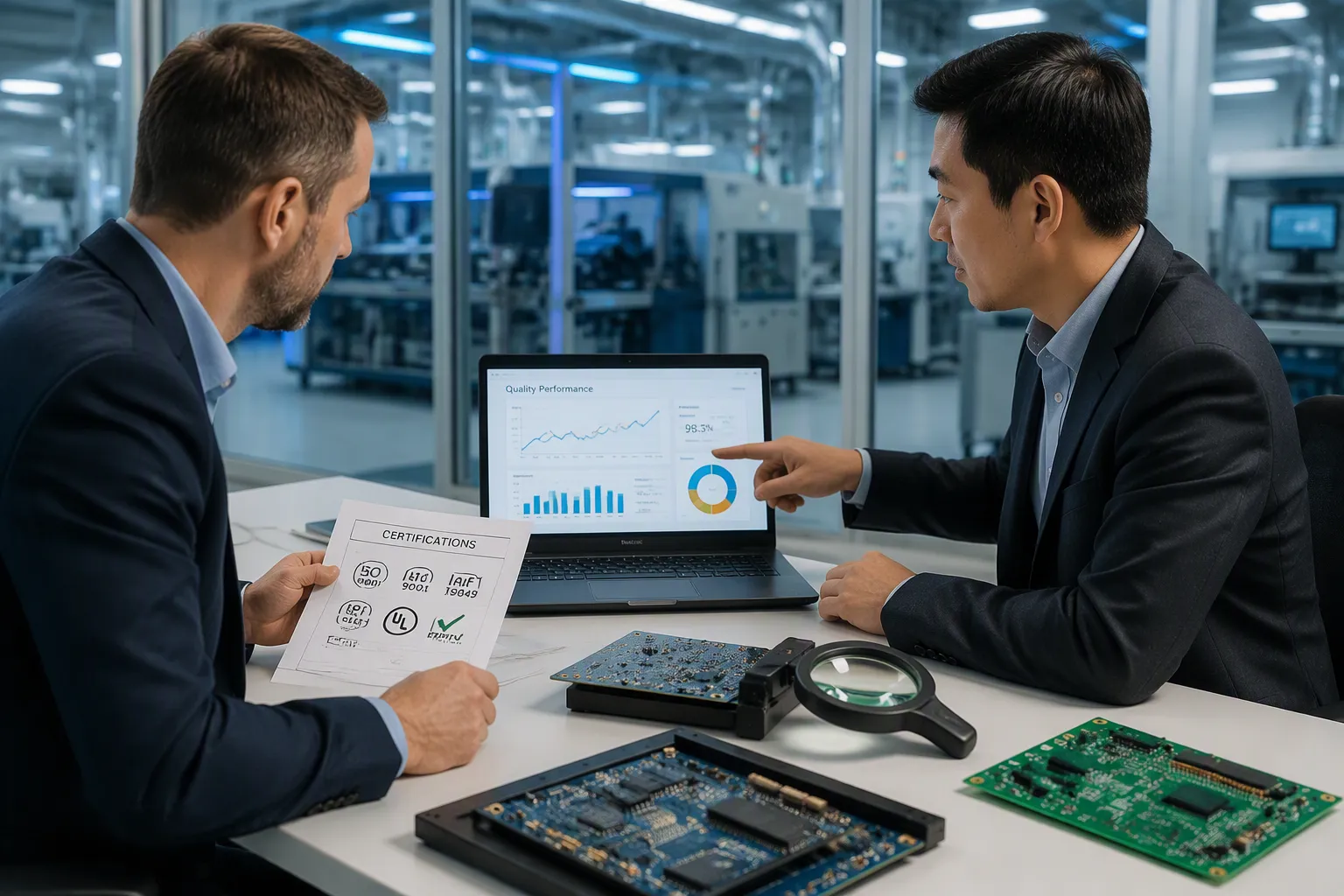
Picking the right factory decides how well your project does. You need a partner who meets technical standards and talks clearly. Start by looking at their credentials and experience in your field. Then check how they handle design review and quoting. Finally, set clear rules for changes, reports, and shipping. This plan stops costly mix-ups.
Key Criteria for Vetting a Factory
Certifications show a factory meets known standards. Each one has a different job. The table below shows what to look for.
Certification | Purpose |
|---|---|
ISO 9001 | Quality management across manufacturing and assembly processes |
IATF 16949 | Automotive-specific quality management (essential for automotive industry) |
UL | Safety compliance for the US market |
RoHS | Environmental compliance for the EU market |
No single certification covers everything. You need a mix that fits your target markets. For car projects, IATF 16949 matters most. For US sales, UL compliance is critical. For EU shipping, RoHS certification is required. Ask to see proof of each certificate. Check that it covers the exact factory location you plan to use.
Experience in your field matters as much as certifications. A factory that builds medical devices knows different rules than one serving consumer electronics. Ask about their past jobs. Request references from clients in your sector. A factory with related experience spots design issues before they turn into production problems.
You should also ask about their AI quality control methods. Request specific details about their inspection algorithms. Ask for recognition accuracy on your target dataset. Inquire about sustained-load stress tests over 48 hours. Verify imaging quality and firmware security. Have a third party like SGS or CTI issue bilingual reports. Ask for chip serial numbers rather than advertised TOPS values. Test actual camera resolution and detection range. These questions show whether their AI claims hold up.
Navigating Communication and Logistics
Clear communication stops most project failures. Start with their DFM review process. A good factory offers a free DFM check before production. They review your Gerber files, BOM, and centroid data. They spot potential assembly issues early. This saves you from costly redesigns later.
Fast quote support also matters. Look for factories that respond within 24 hours. They should provide rapid prototyping and quick-turn assembly. When asking for a quote, send a full package. Include Gerber or ODB++ files, drill files, netlist, fabrication drawing, BOM, centroid data, and commercial inputs like quantities and target dates. A thorough quote covers tooling, fixtures, test time, programming, packaging, and evidence. This ensures the price reflects the full production scope.
One-stop services simplify your supply chain. A single project team coordinates fabrication, sourcing, assembly, inspection, testing, and shipment. This reduces communication gaps. You deal with one contact instead of multiple vendors. For complex boards like an ai hdi pcb, this coordination proves vital. The hdi technology demands precision at every step.
Set clear rules for engineering changes. Define who approves modifications and how quickly they take effect. Set expectations for quality reports. Decide how often you receive inspection data and in what format. Agree on shipping logistics before production starts. Specify Incoterms, packaging standards, and delivery deadlines.
A trusted partner for ai hdi pcbs communicates proactively. They flag potential issues before they escalate. They provide regular updates without you asking. They document every decision and share it openly. This level of communication builds confidence in the partnership.
Working with a factory in china requires patience and structure. You bridge time zones and cultural differences. Clear rules remove confusion. Regular video calls keep everyone aligned. Written summaries after each call prevent misunderstandings. This discipline turns a distant supplier into a reliable extension of your team.
The right partner combines technical excellence with responsive communication. They understand your industry’s demands. They verify their AI claims with real data. They communicate clearly at every stage. This combination delivers consistent quality for your ai devices. You get boards that meet specs, arrive on time, and work reliably in the field. That result justifies the effort you put into selection.
You now see how an AI PCBA factory in China delivers real gains in quality, speed, and cost. Technology alone does not guarantee success. The factory you choose must become a true partner. Start with certifications and industry experience. Set clear rules for engineering changes. Apply ai tools for consistent quality checks. The future of electronics manufacturing belongs to those who combine smart technology with strong partnerships. Apply these principles to your next pcb project. Choose a partner who builds ai devices with precision. Seek a factory that masters hdi design. Your next product deserves this level of commitment for every batch.
FAQ
What minimum order quantity do AI PCBA factories in China require?
Most factories accept both prototypes and volume production. You can start with small batches for testing. Many offer dedicated assembly cells for customer-specific needs. This flexibility lets you validate your design before committing to large orders. Ask each factory for their specific MOQ policy.
How do I verify a factory’s AI inspection claims?
Request specific data about their inspection systems. Ask for recognition accuracy rates on your target dataset. Inquire about sustained-load stress tests over 48 hours. Verify imaging quality and firmware security. Have a third party like SGS or CTI issue bilingual reports. Ask for chip serial numbers rather than advertised TOPS values.
What certifications should an AI PCBA partner hold?
Look for ISO 9001 for quality management. For automotive projects, IATF 16949 matters most. For US sales, UL compliance is critical. For EU shipping, RoHS certification is required. Ask to see proof of each certificate. Check that it covers the exact factory location you plan to use.
How long does prototyping take with an AI-driven factory?
Fast quote support means responses within 24 hours. Rapid prototyping and quick-turn assembly speed up your timeline. The DFM review catches design issues before production starts. This prevents costly redesigns and delays. For complex hdi boards, the automated inspection ensures quality without slowing delivery. Your ai devices reach production faster with this streamlined approach.
See Also
OEM AI PCBA Production For Polish Electronics Plants
Tailored AI PCBA Production For Mexican Electronics Companies
AI Based Inspection PCBA For Mexican Manufacturing Plants