
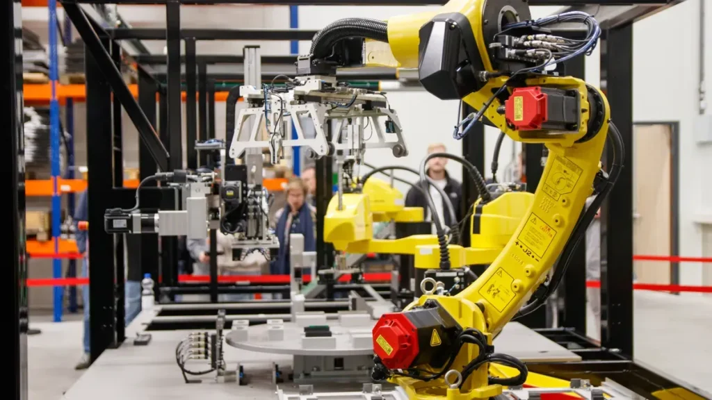
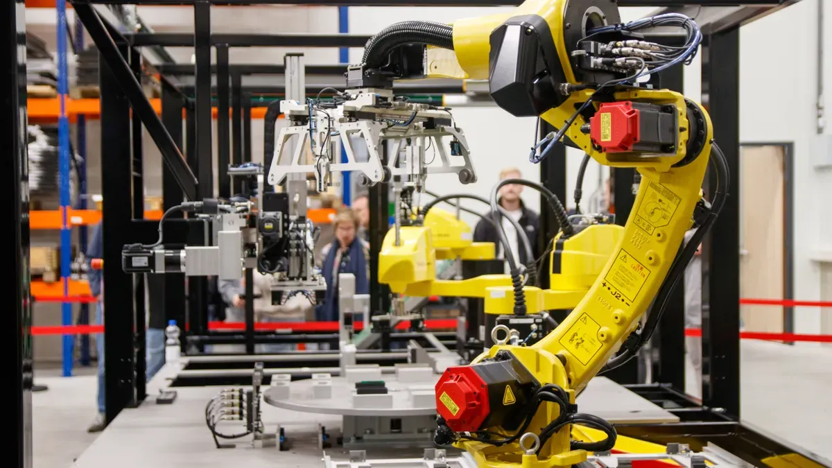
The integration of AI IoT PCB into modern PCBA assembly services plays a crucial role in driving efficiency and innovation. By utilizing AI algorithms, manufacturers streamline production processes, reducing human error and enhancing precision. For instance, PCBA-based surveillance systems have transformed security infrastructure. They utilize high-resolution cameras and intelligent analytics, which significantly improve monitoring capabilities. These advancements allow for proactive detection of security threats, showcasing the innovative applications of AI in the industry.
Key Takeaways
AI IoT technologies enhance efficiency in PCB assembly, reducing errors and improving precision in production processes.
Smart buildings benefit from AI sensors that optimize energy use and indoor environmental quality, leading to significant cost savings.
Small batch production allows for flexibility and customization, making it ideal for startups and niche markets.
BOM kitting streamlines PCB assembly by organizing components, which reduces errors and improves overall productivity.
Functional testing ensures the reliability of PCBA products by validating performance under realistic conditions, minimizing the risk of defects.
AI IoT in Smart Buildings

Applications of AI Sensors
AI sensors play a pivotal role in enhancing the efficiency of smart buildings. They help manage various environmental factors, ensuring optimal conditions for occupants. Here are some key applications of AI sensors in smart building management systems:
Indoor Environmental Quality (IEQ) Management: AI sensors monitor air quality, temperature, and humidity levels, ensuring a comfortable indoor environment.
Energy Consumption Optimization: By analyzing real-time data, these sensors help reduce energy waste, leading to significant savings.
HVAC Optimization: AI sensors adjust heating, ventilation, and air conditioning systems based on occupancy patterns, improving energy efficiency.
Daylighting Control: Sensors can regulate natural light usage, reducing reliance on artificial lighting and further conserving energy.
The systematic literature review indicates a growing adoption of AI technologies in tropical building contexts, particularly in Southeast Asia. These technologies focus on energy efficiency, indoor environmental quality, and space utilization. For instance, sensor-based occupancy data allows building management systems to adjust lighting, ventilation, and temperature based on real-time occupancy, leading to energy savings of 15% to 30%. This not only enhances occupant comfort but also significantly impacts operational costs and environmental footprints.
Role of IoT Gateways
IoT gateways serve as the backbone of smart building automation systems. They integrate various building automation systems, including comfort, lighting, and security services. Here’s how IoT gateways enhance building efficiency:
Integration of Systems: Gateways connect disparate devices into a cohesive Building Automation System (BAS), facilitating better display and reporting.
Real-Time Analytics: They provide analytics that enhance building efficiency and send notifications from critical devices, ensuring timely responses to issues.
Protocol Support: IoT gateways support various protocols, such as BACnet, Modbus, KNX, MQTT, and OPC UA, enabling seamless communication between devices.
The integration of AI IoT in smart buildings not only contributes to sustainability goals but also addresses the increased demand for IoT devices. For example, Bosch’s Singapore office building, equipped with solar panels and smart air conditioning, achieved a 30% reduction in energy consumption compared to similar buildings. Such implementations showcase the potential of AI IoT technologies in transforming building management and operational efficiency.
Small Batch vs. Mass Production in PCB
Characteristics of Small Batch Production
Small batch production in PCB assembly caters to specific market needs. This approach allows you to produce limited quantities of PCBs, which is ideal for prototyping or niche applications. Here are some key characteristics of small batch production:
Flexibility: You can quickly adapt designs based on feedback. This flexibility is crucial during the early stages of product development.
Customization: Small batches allow for tailored solutions. You can modify designs to meet unique customer requirements without the constraints of mass production.
Quality Control: With fewer units produced, you can focus on rigorous quality checks. This ensures that each PCB meets high standards before reaching the market.
However, small batch production also presents challenges. The costs per unit tend to be higher due to the lack of economies of scale. Additionally, the time required for setup and production can be longer compared to mass production.
“Prototype manufacturing focuses on learning and refinement. Engineers expect close monitoring, flexibility, and feedback during early builds. Mass production prioritizes consistency, speed, and cost reduction once the design is stable.”
This quote highlights the importance of understanding the transition from small batch to mass production.
Characteristics of Mass Production
Mass production in PCB assembly is characterized by high efficiency and cost-effectiveness. This method is suitable for large-scale manufacturing, where you can produce thousands of units with minimal variation. Here are some advantages of mass production:
Characteristic/Advantage | Description |
|---|---|
High-frequency performance | Supports higher signal frequencies with lower dielectric loss and tighter tolerances. |
Multilayer and HDI designs | Allows for complex routing, reduces board size, and supports more functionality. |
Rigid-flex and flexible boards | Reduces connectors, saves space, and improves reliability in flexible applications. |
Advanced materials | Higher Tg, lower CTE, and materials optimized for high-frequency performance are in demand. |
Embedded components | Reduces size and improves electrical performance and thermal behavior. |
Innovations in soldering | Ensures reliability in smaller components and mixed technology boards. |
Environmental considerations | Reduces waste and improves recyclability, with technologies like SustainaCircuits™ aiming to cut copper usage significantly. |
Mass production techniques enhance cost efficiency through automation and optimized design processes. High-speed production reduces labor costs and improves quality control. Lower unit costs enable manufacturers to meet increasing demand without compromising quality.
BOM Kitting and SMT in PCBA
Importance of BOM Kitting
BOM kitting is a critical process in PCB assembly. It involves gathering all components needed for production into a single kit. This practice enhances efficiency and reduces errors during assembly. Here are some key benefits of BOM kitting:
Streamlined Production: By organizing components beforehand, you minimize the time spent searching for parts during assembly.
Improved Accuracy: Kitting reduces the risk of missing components, ensuring that each assembly meets design specifications.
Cost Efficiency: With better organization, you can lower labor costs and improve overall productivity.
In the competitive landscape of AI IoT PCB manufacturing, companies like Bonysn have adopted BOM kitting to meet the demands of flexible batch sizes and fast delivery. User reviews highlight how this approach has led to significant improvements in assembly speed and accuracy.
Overview of SMT Techniques
Surface Mount Technology (SMT) plays a vital role in modern PCB assembly. It allows for the efficient placement of components on printed circuit boards. Here are some advancements in SMT techniques that enhance assembly speed and reliability:
Higher Density and Miniaturization: Components are smaller and can be mounted on both sides of the PCB, allowing for more parts in a given area, which is essential for compact AI IoT devices.
Automated, Cost-Effective Production: The use of pick-and-place machines and reflow soldering accelerates assembly, making it less labor-intensive and reducing costs.
Improved Performance: Shorter leads and smaller packages enhance high-frequency signal performance, crucial for the reliability of AI IoT applications.
Advancement Type | Description |
|---|---|
High-Frequency, High-Speed PCBs | Demand for PCBs that support higher signal frequencies, leading to lower dielectric loss and better material choices. |
Multilayer & HDI Designs | More layers enable complex routing and support for compact devices, essential for modern electronics. |
Soldering and Assembly Innovations | New techniques like laser soldering and selective soldering enhance reliability in smaller components. |
The SMT assembly process significantly influences the quality and yield of AI IoT PCB assemblies. Key stages such as solder paste printing, placement, and soldering are critical. Implementing best practices, such as automated optical inspection (AOI), ensures that each board meets stringent quality standards. This rigorous control helps maintain high yield rates and product reliability.
Functional Testing and Shipping for PCBA
Role of Functional Testing
Functional testing plays a crucial role in ensuring the quality and reliability of AI IoT PCBA products. This testing method validates the performance of your assemblies under realistic conditions. It confirms that all critical subsystems, such as power supply and communication interfaces, operate as intended. Here are some key benefits of functional testing:
Validates performance under realistic operating conditions.
Detects latent issues like intermittent failures and timing mismatches.
Confirms that critical subsystems function as intended, ensuring reliability.
The primary advantage of PCB functional testing lies in its ability to validate the board’s performance in realistic usage scenarios. This ensures that defects are detected that other techniques might overlook. Quality assurance protocols during functional testing help reduce failure rates in shipped AI IoT PCBA products. Enhanced test coverage minimizes the risk of undetected issues, while automated testing methods validate the product’s real-world functionality.
Best Practices for Shipping
Shipping PCBA products requires careful planning to ensure they arrive safely and in optimal condition. Here are some best practices to follow:
Use Protective Packaging: Employ anti-static bags and cushioning materials to protect your assemblies from physical damage and electrostatic discharge.
Label Clearly: Ensure all packages are labeled with handling instructions and contents. This helps prevent mishandling during transit.
Choose Reliable Carriers: Partner with reputable shipping companies that have a track record of timely and safe deliveries.
Track Shipments: Utilize tracking systems to monitor the status of your shipments. This allows you to address any issues promptly.
Communicate with Clients: Keep your clients informed about shipping timelines and any potential delays. Transparency builds trust and enhances customer satisfaction.
By implementing these best practices, you can enhance the efficiency of your shipping process and ensure that your PCBA products reach clients in excellent condition.
The integration of AI IoT technologies significantly shapes the future of the PCB assembly industry. You can expect advancements such as:
Smart Manufacturing: Companies like FOZ One leverage AI and IoT for enhanced production efficiency.
Predictive Maintenance: AI systems enable real-time monitoring, reducing downtime.
Increased Connectivity: IoT facilitates seamless communication between machines, improving responsiveness.
As digital transformation accelerates, the demand for semiconductors rises. The growth of smart cities and technologies like cloud computing and 5G drives the need for advanced electronic components. Embracing these trends will position you to meet the evolving needs of Southeast Asia’s AI IoT market effectively.
FAQ
What is AI IoT in smart buildings?
AI IoT in smart buildings refers to the integration of artificial intelligence and Internet of Things technologies to enhance building management. This includes optimizing energy use, improving occupant comfort, and automating systems like lighting and HVAC.
How does BOM kitting improve PCB assembly?
BOM kitting organizes all necessary components for PCB assembly into a single kit. This streamlines production, reduces errors, and enhances efficiency, allowing for faster assembly and improved accuracy in meeting design specifications.
What are the benefits of functional testing in PCBA?
Functional testing validates the performance of PCBA products under realistic conditions. It ensures that all critical subsystems operate correctly, helping to detect issues that might be missed by other testing methods, thus enhancing product reliability.
Why is small batch production important for startups?
Small batch production allows startups to test and refine their designs without committing to large quantities. This flexibility helps you adapt quickly to market feedback and customize products to meet specific customer needs.
How can I ensure safe shipping of PCBA products?
To ensure safe shipping, use protective packaging like anti-static bags and cushioning materials. Clearly label packages with handling instructions and choose reliable carriers to minimize the risk of damage during transit.
See Also
Comprehensive AI PCBA Solutions for Singapore’s IoT and MedTech
Tailored AI PCBA Production for Electronics Firms in Mexico
Original Equipment Manufacturer AI PCBA for Belgian Tech Firms