
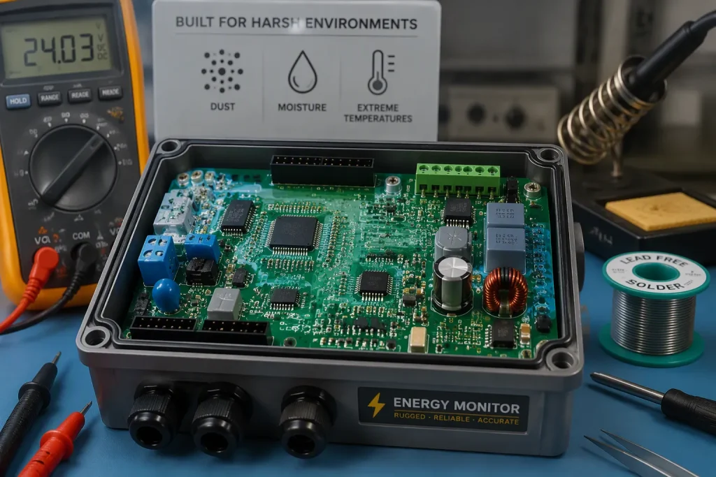
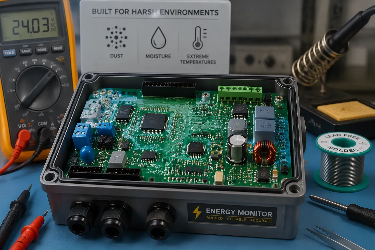
Designing an energy monitoring PCBA for harsh environments demands careful planning. You must balance measurement accuracy against extreme temperatures, humidity, vibration, and electrical transients. Applications include photovoltaic monitoring in desert solar farms, energy storage management, mining equipment, and outdoor communication terminals.
Consider a steel-mill switchgear cabinet. A field failure from thermal runaway or signal drift halted production for hours. The cost of that downtime far exceeded the price of a robust PCB assembly.
Your power supply design determines survival. Surge protection, ESD safeguards, and reverse polarity protection form your first defence. Thick copper PCB layers handle high currents while dissipating heat effectively. This energy monitoring PCBA approach prevents costly failures.
Every assembly decision affects reliability. Component selection, solder quality, and conformal coating protect against dust and moisture. Your energy PCBA assembly must withstand years of operation. The power budget, monitoring accuracy, and PCB layout all contribute to success. A well-designed energy monitoring PCBA delivers dependable data for decades. This PCBA must also handle power surges without compromising accuracy. Your energy monitoring PCBA assembly requires careful PCB testing.
Key Takeaways
Design your energy monitoring PCBA to survive extreme temperatures, humidity, and vibration.
Use surge protection, reverse polarity protection, and thick copper layers for reliable power delivery.
Select precision components and apply conformal coating to resist moisture and dust.
Validate your design with thermal cycling and vibration testing before mass production.
Environmental Demands and Application Contexts
Temperature, Vibration, and Humidity Challenges
Your energy monitoring PCBA must survive conditions that would destroy standard electronics. Temperature swings from -40°C to +85°C stress solder joints and cause materials to expand and contract at different rates. This thermal cycling eventually cracks connections and degrades measurement accuracy.
Humidity presents an equally serious threat. High humidity causes a thin film of water to form on metal surfaces, enabling electrochemical corrosion where metal atoms dissolve and react with oxygen. Temperature swings in tropical environments cause warm, humid air to condense on cooler PCBA surfaces, directly forming moisture. For copper traces common in circuit boards, the critical relative humidity sits at 55-60%. Above this level, corrosion accelerates rapidly. Salt contamination from coastal installations can lower this threshold to as little as 34% RH, making even moderately humid air dangerous.
Vibration adds another layer of complexity. Mining equipment generates constant mechanical shock that loosens connectors and fatigues solder joints over time. Your PCB layout must account for these forces through proper component placement and mechanical reinforcement.
Application | Primary Challenge | Critical Risk |
|---|---|---|
Desert solar farm | Extreme heat, UV exposure | Thermal degradation, signal drift |
Mining equipment | Dust, vibration, impact | Connector failure, solder fatigue |
Outdoor telecom | Rain, ice, salt fog | Corrosion, moisture ingress |
Solar, Mining, and Outdoor Telecom Applications
Photovoltaic monitoring in desert solar farms demands exceptional heat tolerance. Your energy monitoring PCBA sits inside enclosures that absorb direct sunlight, pushing internal temperatures well beyond ambient levels. High-current paths generate additional heat, so thermal management becomes essential for maintaining measurement stability.
Mining equipment presents a different challenge. Dust infiltrates every gap, while constant vibration tests the integrity of every connection. You need robust enclosures and conformal coating to protect the PCB from abrasive particles. Maintenance access is difficult underground, so reliability directly affects operational uptime.
Outdoor telecom terminals face rain, ice, and coastal salt fog. For offshore installations, manufacturers recommend Silicone Resin (SR) conformal coating because it provides good salt spray resistance and moisture protection. This coating forms a barrier that keeps corrosive elements away from sensitive components.
These applications share common requirements: stable power delivery, reliable connections, and thermal management. An IoT gateway for energy monitoring deployed in any of these environments demands the same rugged design principles. Your industrial energy monitoring system must deliver accurate data despite these harsh conditions. The monitoring accuracy you achieve depends entirely on how well you address these environmental factors during the design phase.
Power Supply and Protection for Energy PCBA Assembly
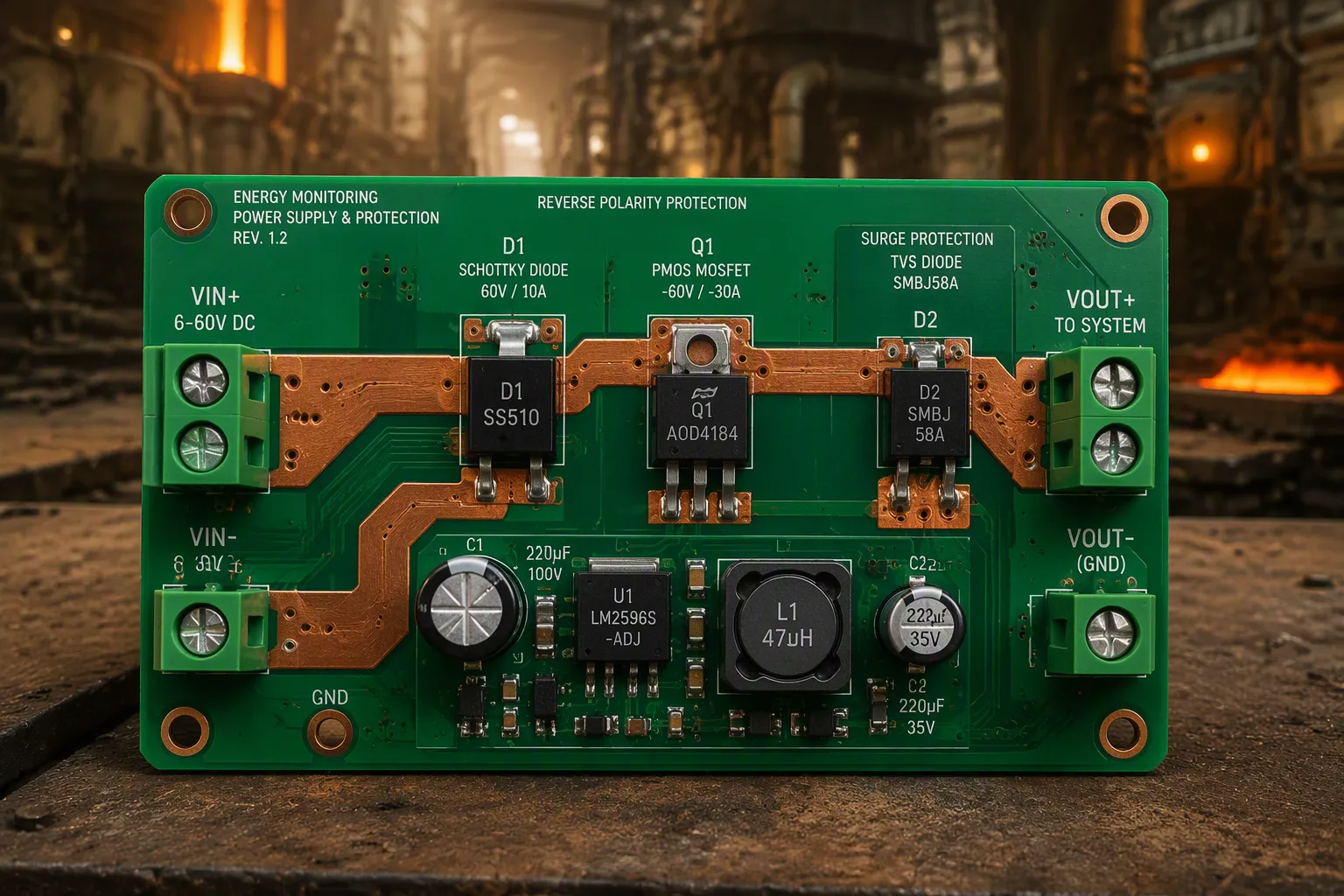
Your power supply design determines the survival of an energy monitoring PCBA in harsh environments. You need protection circuits that handle surges, electrostatic discharge, and reverse polarity without fail. Thick copper PCB layers manage heat in high-current paths. Let us examine each layer of protection.
Surge, ESD, and Reverse Polarity Protection
Start with transient protection at the power entry point. A TVS diode absorbs surge from lightning strikes or switching events. Three parameters guide your selection.
Parameter | Definition |
|---|---|
Standoff voltage (Vwm) | Maximum continuous voltage the device can withstand without significant conduction. Must be above circuit’s normal operating voltage. |
Clamping voltage (Vc) | Maximum voltage across the device during a specified peak pulse current condition. Determines the voltage level the protected circuit will see. |
Peak pulse current (Ipp) | Maximum transient current the device can absorb without damage, typically specified for a given waveform (e.g., 8/20 µs). Related to peak pulse power (Ppp = Vc * Ipp). |
Choose a TVS with a clamping voltage below your downstream components’ rating.
Ground-loop interference creates erratic readings on your power monitoring circuit board. When AGND and DGND cross a split on the PCB bottom layer, sampled values jump erratically. You can see accuracy drift of around 0.8 per cent on a Class 0.2 channel. Keep analog and digital ground planes separate and connect them at a single star point.
Reverse polarity protection prevents damage from incorrect battery connections during installation. You have two common options. A Schottky diode offers simple protection but creates a forward voltage drop that reduces output voltage. Power dissipation remains constant as load current flows through the diode. A PMOS MOSFET provides a better solution for high-current applications.
Parameter | Schottky Diode | PMOS MOSFET |
|---|---|---|
Voltage Drop | Forward voltage drop reduces output voltage below input | Minimal voltage drop due to low RDS(on) in milliohms |
Power Dissipation | Constant power loss from load current flowing through diode | Lower power dissipation due to low on-resistance |
Efficiency | Inefficient for high-current applications | More efficient, suitable for high-current applications |
Circuit Behavior | Blocks reverse current but wastes energy | Turns off during reverse polarity, disconnects positive rail safely |
A fuse or PTC resettable device adds overcurrent protection in the power path. Place it after the reverse polarity protection circuit.
Power supply ripple coupling causes noise in your measurements on an energy monitoring PCBA. Switching harmonics at 100 kHz and mains interference at 50 Hz enter the analog front end, reducing effective bits below 20. Place decoupling capacitors close to ADC pins. A capacitor placed half an inch from the pin fails to filter ripple effectively.
Thick Copper PCBs for Thermal Management
High-current paths in your energy monitoring PCBA generate significant heat. A standard 1 oz copper PCB cannot handle the current without excessive temperature rise. You need thick copper PCB layers from 2 oz to 4 oz or more. These thicker layers reduce resistive losses and improve thermal dissipation.
Failure Mode | Root Cause / Contributing Factor | Impact on Grid Monitoring |
|---|---|---|
Surge-induced reboot | Lack of transient protection at power entry (TVS diode, common-mode inductor) | Data loss, unit downtime |
Ground-loop interference | AGND and DGND crossing a split on the PCB bottom layer | Sampled values jump erratically; accuracy drift (e.g., 0.8% off on a Class 0.2 channel) |
Power supply ripple coupling | 100 kHz switching harmonics and 50 Hz mains interference entering analog front end | Reduced effective bits (below 20), noisy measurements |
Decoupling capacitor misplacement | Capacitors placed half-inch from ADC pins, power not routed through them | Ripple pours into sampling loop, causing inexplicable noise |
LDO PSRR degradation | LDO’s power supply rejection ratio drops at switching frequency | Sampled numbers become unreliable even with 24-bit ADC |
For EV charger modules and grid monitoring equipment, thick copper PCB prevents hotspots that degrade measurement accuracy. The lower resistance means less voltage drop across the PCB. Your power monitoring design benefits from this approach because the voltage sense lines on the PCB see a cleaner reference.
LDO PSRR degradation creates another challenge. An LDO’s power supply rejection ratio drops at switching frequency, making sampled numbers unreliable even with a 24-bit ADC. Thick copper PCB helps by reducing impedance in the power distribution network, maintaining cleaner supply rails.
Your PCB assembly process must handle thick copper boards correctly. The etching process during assembly differs from standard boards. Solder paste application during assembly requires careful control to achieve proper joint formation. An experienced assembly partner like bonysn understands these nuances.
Your PCB layout must also consider component placement for your energy monitoring PCBA. During assembly, keep high-current components away from sensitive analog circuitry. Use thermal vias on the PCB to conduct heat to inner layers or the opposite side of the board.
Design and Assembly for Energy Monitoring PCBA
Component Selection and PCB Layout
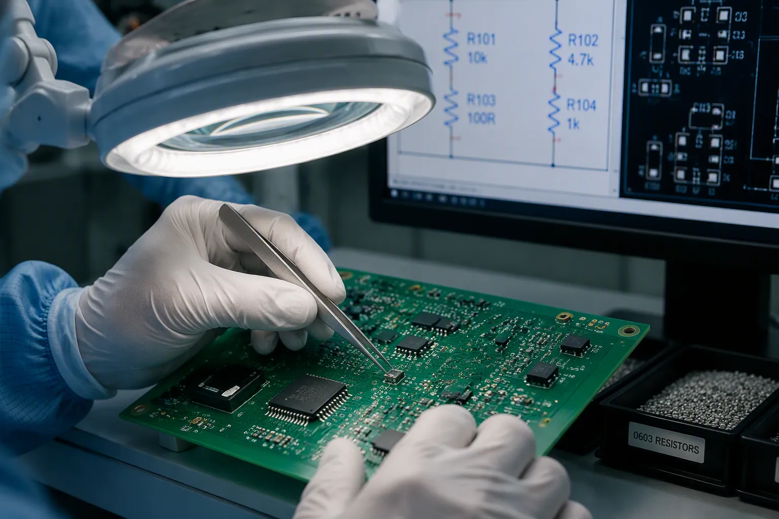
Your component choices determine whether your energy monitoring PCBA survives years of harsh service. Precision resistors form the backbone of accurate current sensing. You need low tolerance parts, typically 0.5% or 1.0%, to maintain measurement accuracy. Temperature coefficient matters equally. A resistor that drifts with temperature corrupts your readings long before any other component fails.
Use Kelvin sensing, also known as 4-terminal measurement, to eliminate connection resistance errors. This technique separates current-carrying and voltage-sensing paths. The Vishay WSK series exemplifies this approach, removing trace resistance from your measurement loop entirely. Thermal EMF presents another subtle error source. The Vishay WSL series generates only 3µV/°C, compared to ±25µV/°C from competitors. In low-voltage sensing applications, this difference prevents microvolt-level errors from corrupting your data.
Match resistor values to your expected current range. Small values, in the hundredths or thousandths of an ohm, suit low-power applications. They minimise power loss while maintaining adequate signal strength for your ADC.
PCB layout demands equal attention. Creepage distance, the shortest path between two conductive parts along a surface, must meet clearance requirements for your operating voltage. Contamination from dust or moisture reduces effective creepage, so you need generous spacing in harsh environments. Signal isolation prevents ground loops from corrupting measurements. Galvanic isolation using digital isolators blocks common-mode voltage differences between your RS485 transceiver and microcontroller. This protection stops ground loops from destabilising logic circuits.
Technique | EMI Prevention Function |
|---|---|
Galvanic isolation (digital isolators) | Blocks common-mode voltage differences between RS485 transceiver and microcontroller, preventing ground loops and protecting the processor |
Isolated DC-DC converter (≥1.5kV isolation) | Prevents ground loop currents from destabilising logic circuits and corrupting ADC readings |
Pi-filter (ceramic capacitors + common-mode choke) | Blocks high-frequency electromagnetic noise from entering the power network |
Gas Discharge Tubes (GDTs) | Shunts high-energy surges directly to chassis earth, preventing transient damage to sensitive circuits |
An IoT gateway for energy monitoring deployed in an industrial setting benefits directly from these techniques. The RS485 bus carries data across long distances, often through electrically noisy environments. Without proper isolation, you risk corrupted communication and intermittent failures.
Grounding strategy completes your layout. Separate analog and digital ground planes, then connect them at a single star point. This arrangement prevents digital switching noise from contaminating sensitive analog measurements. Your power monitoring circuit board will deliver cleaner data when you follow this discipline.
SMT Assembly and Conformal Coating
Your PCB assembly process transforms the design into a physical product. Surface mount technology (SMT) handles the majority of components. Through-hole technology (THT) remains necessary for large connectors and components that endure mechanical stress. Your assembly partner must manage both processes with precision.
Solder joint quality determines long-term reliability. Poor wetting, insufficient solder volume, or cold joints fail under thermal cycling. IPC-A-610 Class 2 acceptance criteria provide a benchmark for industrial electronics. Class 3, for high-reliability applications, demands even stricter standards. Your energy monitoring PCBA deserves at least Class 2 compliance.
Assembly Parameter | Standard Practice | bonysn Capability |
|---|---|---|
Solder paste application | Stencil printing with controlled thickness | Precision stencil alignment for fine-pitch components |
Reflow profiling | Temperature curve matched to solder alloy | Real-time profiling for consistent joint formation |
Inspection | AOI after reflow, X-ray for BGA | Automated optical inspection on every board |
Conformal coating | Selective spray or dip application | Programmable selective coating for precise coverage |
Conformal coating protects your PCB from humidity, dust, and corrosive gases. Mining equipment and outdoor telecom terminals demand this protection. Acrylic coatings offer good moisture resistance and easy rework. Silicone resin coatings provide superior salt spray resistance for coastal installations. Polyurethane coatings resist solvents and abrasion. Your choice depends on your specific environment.
The coating process requires careful masking. Connectors, test points, and calibration areas must remain exposed. A programmable selective coating system applies material precisely, avoiding these areas automatically. Your assembly partner should demonstrate this capability.
Your PCB assembly process must also handle thick copper boards correctly. The etching process differs from standard boards. Solder paste application requires careful control to achieve proper joint formation. An experienced assembly partner like bonysn understands these nuances.
Thermal management during assembly prevents damage to sensitive components. Reflow profiles must match the solder alloy specification. Slow ramp rates reduce thermal stress on ceramic capacitors and precision resistors. Your assembly partner should document their reflow profile for each product.
Functional testing after assembly verifies that your energy monitoring PCBA meets specifications. In-circuit testing checks individual components. Boundary scan testing verifies digital connections. Calibration adjusts gain and offset errors in measurement channels. Your assembly partner should offer these services to ensure your boards perform correctly.
The combination of careful component selection, disciplined layout, and controlled assembly produces an energy PCBA assembly that survives harsh environments. Your monitoring accuracy depends on every step of this chain. A single weak link compromises the entire system.
Testing and Reliability for Rugged PCBA
Thermal Cycling and Reliability Testing
You cannot trust an energy monitoring PCBA until you prove it survives real-world conditions. Thermal cycling testing pushes your board through repeated temperature extremes, typically from -40°C to +85°C for 100 cycles. This test reveals weak solder joints, cracked components, and material mismatches before your equipment reaches the field. Each cycle expands and contracts materials at different rates, exposing any design flaw.
Highly Accelerated Life Testing (HALT) takes a different approach. You gradually increase stress levels—temperature, vibration, voltage—until failures occur. This method identifies your design’s actual limits rather than just confirming it meets specifications. You learn where your weak points sit, then strengthen them before mass production.
Vibration testing simulates years of mechanical stress in hours. Your energy monitoring PCBA must endure the constant shaking found in mining equipment or near heavy machinery. Random vibration profiles replicate real-world conditions more accurately than simple sine sweeps. You should test with fixtures that mimic your actual mounting method.
Test Method | Purpose | Key Parameter |
|---|---|---|
Thermal Cycling | Reveal solder joint fatigue | -40°C to +85°C, 100 cycles |
HALT | Find design limits | Increasing stress until failure |
Vibration | Simulate mechanical stress | Random profile, mounted fixture |
Functional Testing and Compliance
Automated Optical Inspection (AOI) scans every board after assembly. This system checks solder joint quality, component placement, and polarity markings. You catch manufacturing defects before they become field failures. In-Circuit Testing (ICT) goes further, verifying each component’s electrical performance individually.
Calibration accuracy matters most for your energy monitoring PCBA. You must verify that voltage and current readings stay within tolerance across the full operating range. Isolation testing confirms that your galvanic barriers withstand specified voltages without breakdown. Your assembly partner should document these results for every batch.
Compliance standards provide your quality benchmark. IEC 61000 covers electromagnetic compatibility, ensuring your board neither emits excessive interference nor suffers from external noise. IEC 62052 applies specifically to metering equipment, defining accuracy requirements for energy measurement. UL 61010 addresses safety, protecting operators from electrical hazards. A high reliability PCBA meets all three standards.
Your assembly partner should offer these tests as standard services. bonysn provides complete testing documentation with every batch, giving you traceability from component sourcing through final verification. This documentation proves your energy monitoring PCBA meets specification before installation.
Your energy monitoring PCBA success starts with understanding environmental demands. Design robust power supply protection with surge and ESD circuits. Use thick copper PCB layers for thermal management. Select precision components. Validate your energy monitoring PCBA through rigorous testing. Partner with a reliable PCBA manufacturer like bonysn. They understand harsh environment requirements. Your energy monitoring PCBA design prevents costly field failures. Consult a specialist for your next energy PCBA assembly project. Assembly precision ensures reliable data. Your PCB layout choices directly affect long-term success. This approach delivers dependable monitoring equipment for demanding applications.
FAQ
Which conformal coating suits my application best?
Your choice depends on your operating environment. Acrylic coatings offer good moisture resistance and easy rework. Silicone resin provides superior salt spray protection for coastal sites. Polyurethane resists solvents and abrasion. For mining dust and vibration, acrylic offers a balanced solution. For offshore telecom, choose silicone resin.
Coating Type | Moisture Resistance | Salt Spray Resistance | Rework Difficulty |
|---|---|---|---|
Acrylic | Good | Moderate | Easy |
Silicone Resin | Excellent | Excellent | Difficult |
Polyurethane | Good | Good | Moderate |
What standards must my energy monitoring PCBA meet?
Your energy monitoring PCBA should comply with three key standards. IEC 61000 covers electromagnetic compatibility. IEC 62052 defines accuracy requirements for metering equipment. UL 61010 addresses operator safety. Together, these standards ensure your board performs reliably in harsh conditions. Your assembly partner should document compliance for every batch.
How does bonysn ensure quality for harsh environments?
Bonysn applies IPC-A-610 Class 2 acceptance criteria as a minimum benchmark. They perform automated optical inspection on every board. Their programmable selective coating system masks connectors and test points precisely. They document reflow profiles for each product. This approach delivers consistent solder joint quality across production runs.
Does rugged assembly cost more than standard production?
Yes, but the premium is modest compared with field failure costs. Thick copper PCB layers, conformal coating, and additional testing add expense. A steel-mill failure from thermal runaway can halt production for hours. The downtime cost far exceeds the assembly premium. You protect your operational uptime by investing in robust assembly.
How do I validate my design before mass production?
You should request thermal cycling testing from -40°C to +85°C for 100 cycles. Highly Accelerated Life Testing (HALT) identifies your design’s actual limits. Vibration testing simulates years of mechanical stress. Bonysn provides complete testing documentation with every batch. This traceability proves your energy monitoring PCBA meets specification before installation.
See Also
Durable AI Circuit Boards for Norwegian Sea and Power Monitoring
Sturdy Edge AI Boards for Canadian Outdoor Surveillance Systems
Robust AI Circuitry for Australian Mining and Power Sectors
Edge AI Board Assembly for Canadian Visual and Tracking Equipment
AI Sensor Circuit Boards for Dutch Horticulture and Chip Machinery