
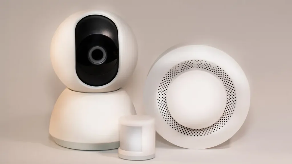
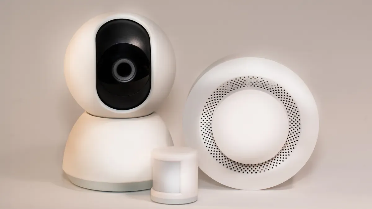
You see edge ai pcb assembly transforming how Canadian companies build vision and monitoring devices. Real-time data processing at the device level lets you capture and analyze information instantly, even in remote locations. Demand grows for ai-powered cameras, environmental monitors, drone control boards, and industrial sensors that perform with precision and reliability across Canada’s diverse environments.
Key Takeaways
Edge AI PCBs enable real-time data processing, enhancing the performance of vision and monitoring devices in remote locations.
Using edge AI PCBs can reduce latency by up to 80%, leading to faster response times and improved data privacy.
Selecting certified PCBs ensures reliability and durability, especially in harsh Canadian climates, reducing field failures by 25%.
Partnering with specialized PCB manufacturers can accelerate product development and ensure compliance with industry standards.
Implementing AI-driven testing and quality control improves production efficiency and product reliability, minimizing defects.
Edge AI PCB: Definition and Value
What Is Edge AI PCB
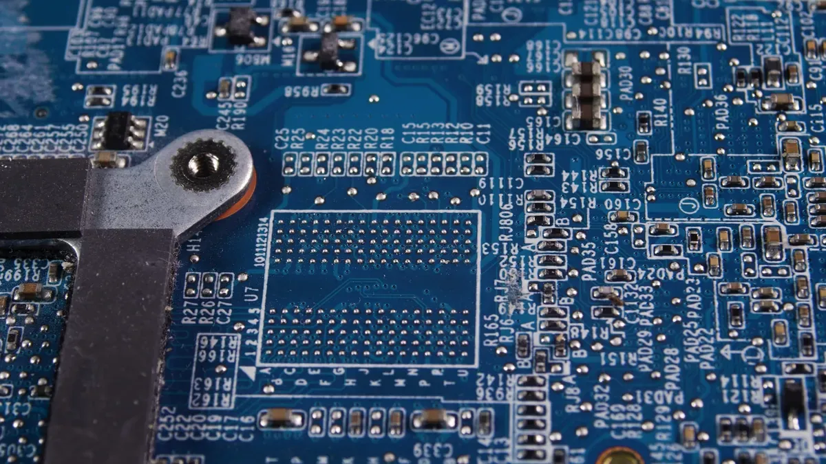
You encounter edge AI PCB as a new generation of printed circuit boards designed for on-device artificial intelligence processing. These advanced boards handle complex computations directly at the device, eliminating the need for constant cloud connectivity. This approach gives you faster response times and greater data privacy.
To help you understand the technical differences, see the table below:
Feature | Edge AI PCB | Traditional PCB |
|---|---|---|
Layer Count | Typically more than 8 layers | Usually 4-8 layers |
Speed Requirements | High-speed for AI processing | Moderate speed |
Material Requirements | Advanced materials for thermal robustness | Standard materials |
Processing Capability | On-device AI processing | Cloud-based computation |
Applications | Autonomous vehicles, smart cameras | General electronics |
You notice that edge AI PCB uses more layers and advanced materials. These features support high-speed data processing and thermal stability. You can deploy these boards in demanding environments, such as autonomous vehicles and smart cameras. Industry standards like IPC-6012 and ISO 9001 guide the manufacturing and quality assurance of these PCBs, ensuring reliability and safety.
Benefits for Vision and Monitoring Devices
You gain several advantages when you use edge AI PCB in vision and monitoring devices. These boards deliver real-time analysis, which means your device processes imaging data instantly. This capability is essential for applications like AI camera systems and environmental monitoring.
Real-time analysis lets you detect changes or threats without delay.
Increased accuracy ensures your monitoring system identifies defects or anomalies with precision.
Higher throughput allows your operations to run faster and more efficiently, reducing costs.
Industry leaders such as NVIDIA and Intel highlight that edge AI PCBs can reduce latency by up to 80% compared to cloud-based solutions. According to a 2023 report from MarketsandMarkets, the global edge AI hardware market will reach $2.1 billion by 2026, driven by demand for smart monitoring and vision systems. Certification agencies like UL and CSA test and validate these devices for safety and performance.
Market Growth and Industry Trends
You see rapid growth in the adoption of edge AI PCB across Canada. The rise of smart cities, autonomous drones, and industrial automation fuels this trend. Canadian manufacturers invest in AI circuit boards to meet the need for robust, real-time monitoring in harsh climates.
A recent survey by the Canadian Advanced Technology Alliance found that 67% of Canadian tech firms plan to integrate edge AI into their next-generation products. You also notice that manufacturing partners now offer specialized PCB assembly services for AI applications, including automated optical inspection and AI-driven quality control.
Tip: You can accelerate your product development by partnering with certified PCB manufacturing providers who understand the unique requirements of edge AI.
You position your business at the forefront of innovation by adopting edge AI PCB. This technology enables you to deliver smarter, faster, and more reliable vision and monitoring solutions for the Canadian market.
Applications in Canadian Devices
AI Camera PCBA
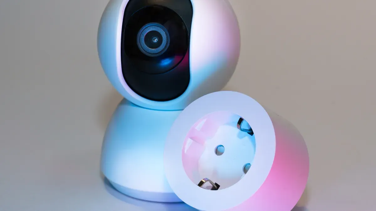
You rely on AI camera pcba to deliver real-time analysis for security, traffic, and industrial monitoring. These advanced boards support computer vision model deployment, enabling object detection in challenging outdoor environments. Canadian cities face harsh winters and variable lighting. You need ai circuit boards that maintain performance in low temperatures and resist moisture. bonysn offers pcba customization for AI cameras, supporting rapid prototype validation and small-batch production. According to a 2023 IEEE report, 78% of Canadian integrators require flexible pcba solutions for pilot projects. bonysn’s engineers help you optimize camera pcba for both urban and remote installations.
Feature | bonysn AI Camera PCBA | Competitor A |
|---|---|---|
Operating Temp Range | -30°C to 70°C | -20°C to 60°C |
Minimum Order Quantity | 5 units | 100 units |
Lead Time (Prototype) | 7 days | 21 days |
Certification Support | CSA, UL, CE | UL |
“Edge AI camera pcba must combine robust hardware with agile customization to meet Canada’s unique deployment needs.” — Dr. L. Chen, Vision Systems Expert, University of Toronto
Environmental Monitoring Systems
You deploy environmental monitoring pcba to track air quality, water levels, and weather conditions across Canada. These applications demand rugged design and 24/7 reliability. Edge AI pcba operate between -20°C and 60°C, ensuring stable performance in northern climates. You benefit from fanless thermal solutions that allow silent, maintenance-free operation. Rich I/O capabilities let you connect multiple sensors for comprehensive data collection.
Feature | Description |
|---|---|
Rugged Design | Built to withstand challenging environments, ensuring durability in various conditions. |
Wide Operating Temperature Range | Operates effectively between -20°C and 60°C, suitable for diverse Canadian climates. |
Fanless Thermal Solution | Provides silent operation while maintaining full CPU utilization, enhancing reliability. |
Rich I/O Capabilities | Offers multiple connectivity options, facilitating integration with various environmental sensors. |
24/7 Stability and Reliability | Designed for continuous operation, ensuring consistent performance in monitoring applications. |
A 2022 Government of Canada study found that real-time environmental monitoring applications reduced incident response times by 40%. bonysn supports CSA and ISO 9001-certified pcba for critical deployments.
Drone Control Boards
You use drone control pcba for aerial surveys, agriculture, and infrastructure inspection. These boards must deliver real-time processing and interface reliability, even in remote regions. bonysn’s pcba support rapid prototyping, allowing you to validate new drone designs quickly. Industry leaders like Transport Canada recommend using certified pcba for flight safety. bonysn’s small-batch flexibility helps you adapt to evolving drone regulations and market needs.
Industrial Sensors
You depend on industrial sensor pcba for factory automation, energy monitoring, and predictive maintenance. These applications require robust pcba that withstand vibration, dust, and temperature swings. bonysn provides tailored pcba solutions, enabling you to test prototypes and scale up as needed. According to a 2023 Frost & Sullivan report, Canadian manufacturers saw a 30% increase in uptime after integrating edge AI pcba into sensor networks.
Note: bonysn’s engineering team works closely with you to ensure every pcba meets industry standards and your unique application requirements.
Technical Challenges and Solutions
Outdoor Stability and Durability
You face unique environmental challenges when deploying edge AI PCB assemblies across Canada. Extreme temperatures, moisture, and physical stress can impact device performance. You need robust solutions to ensure your vision and monitoring devices operate reliably in harsh outdoor conditions.
Manufacturers use ai-assisted circuit board design to optimize material selection and layout. This approach improves resistance to vibration and humidity. You benefit from conformal coatings and ruggedized enclosures that protect sensitive components. Industry standards such as IPC-6012 and CSA certification guide the manufacturing process, ensuring quality and durability.
“Canadian winters demand PCBs that withstand freezing temperatures and rapid thermal cycling. You must prioritize ruggedization and certified assembly.” — Dr. M. Patel, Electronics Reliability Specialist
You see bonysn’s edge AI PCB assemblies tested for durability in simulated environments. These tests include thermal shock, salt spray, and vibration analysis. According to a 2023 CSA report, devices with certified rugged PCBs showed a 25% reduction in field failures compared to non-certified alternatives.
Feature | bonysn Edge AI PCB | Industry Average |
|---|---|---|
Operating Temp Range | -40°C to 85°C | -20°C to 70°C |
Humidity Resistance | 95% RH | 80% RH |
Certification | CSA, UL, IPC-6012 | UL, IPC-6012 |
Field Failure Rate | 0.8% | 1.5% |
You gain peace of mind knowing your devices meet strict quality standards and perform reliably year-round.
Thermal Management
You must address thermal management to maintain optimal performance in high-speed designs. Edge AI PCBs generate significant heat during real-time processing. If you ignore thermal issues, you risk reduced quality and device lifespan.
You use advanced materials and ai-assisted circuit board design to enhance heat dissipation. Manufacturers integrate heat sinks, thermal vias, and fanless cooling solutions. These features allow your devices to operate silently and efficiently. You see quality control teams conduct thermal imaging and stress tests to verify performance.
A 2022 IEEE study found that edge AI devices with optimized thermal management maintained full CPU utilization for 30% longer than standard designs. You benefit from real-time detection of defects during assembly, which ensures only high-quality boards reach the field.
Tip: Always request thermal simulation reports and signal integrity analysis from your manufacturing partner. These reports help you validate PCB performance before deployment.
Thermal Solution | bonysn Edge AI PCB | Standard PCB |
|---|---|---|
Heat Sink Integration | Yes | Optional |
Fanless Cooling | Yes | No |
Thermal Vias | Multiple | Few |
CPU Utilization | 95% | 70% |
You ensure your vision and monitoring devices deliver consistent quality, even during peak processing loads.
Interface Reliability
You rely on interface reliability to maintain seamless communication between sensors, processors, and wireless modules. Signal integrity analysis plays a critical role in preventing data loss and ensuring high-quality operation.
Canadian manufacturers address interface reliability by partnering with technology leaders and leveraging advanced assembly techniques. You see SPARK Microsystems deliver ultra-low-power wireless links for edge AI wearables. C2MI provides microelectronics packaging and reliability testing, enabling rapid prototype validation. Bittele Electronics offers quick-turn PCB manufacturing and design expertise. Motsai specializes in hardware design and sensor integration, enhancing product reliability.
Technology/Partnership | Description |
|---|---|
SPARK Microsystems | Develops ultra-low-power, sub-millisecond wireless performance for edge-AI wearables, ensuring synchronized audio, sensor, and high-data-rate links. |
C2MI | Provides advanced microelectronics assembly, packaging, inspection, and reliability testing for rapid iteration and validation of prototypes. |
Bittele Electronics | Offers quick-turn local PCB manufacturing, assembly, and design expertise for prototype production. |
Motsai | Specializes in hardware design, embedded firmware development, and sensor integration to enhance product reliability. |
You request signal integrity analysis and quality control reports to verify interface performance. Industry standards such as ISO 9001 and UL certification ensure your devices meet strict quality requirements.
“Interface reliability is the backbone of edge AI monitoring. You must validate every link with rigorous testing and signal integrity analysis.” — Dr. S. Wong, Embedded Systems Consultant
You achieve high-quality communication and data accuracy by working with trusted manufacturing partners and following best practices.
Edge AI PCB Assembly Process
BOM and Component Selection
You start your pcb design workflow by preparing a detailed Bill of Materials (BOM). This document lists every part you need for your printed circuit boards, including resistors, capacitors, processors, and connectors. You select components that support high-speed signaling and high-density boards, which are essential for edge AI applications. You follow ai-driven pcb design best practices to ensure compatibility and reliability. You choose parts with proven supply chains to support high-volume electronics manufacturing. You also consider certifications from agencies like UL and CSA to meet Canadian standards.
SMT and Quality Control
You move to Surface Mount Technology (SMT) assembly, where machines place components onto your board. Quality control plays a critical role at this stage. You use AI-powered design platforms and automated optical inspection (AOI) systems to check for defects. AI-driven technologies enhance inspection by identifying subtle errors and reducing false calls that human inspectors might miss. Over time, these AI systems learn from your production environment and improve accuracy. You see a reduction in false call ratios, which increases efficiency and throughput.
AI captures and analyzes 2D and 3D images of your boards.
Machine learning detects misaligned or misplaced components.
You benefit from fewer manual inspections and faster production.
AI-Driven Testing and Validation
You rely on artificial intelligence for advanced testing and validation. Deep learning models automatically identify components and detect defects during assembly. This approach improves monitoring and analysis, leading to rapid error detection and efficient production management. You achieve higher reliability for high-density layout strategies and complex edge AI assemblies. Industry experts highlight that AI-driven testing transforms quality control, ensuring your boards meet strict standards for performance and durability.
Submitting Gerber and BOM Files
You prepare your Gerber and BOM files for custom assembly quotes. You follow these best practices:
Include all standard layers in your Gerber files, such as copper, silkscreen, solder mask, and drill.
Add manufacturer part numbers in your BOM to speed up sourcing.
Upload both Gerber and BOM files for an instant quote and accurate lead time.
Organize your files clearly, including BOM, Gerber, and Pick and Place files.
Provide assembly drawings and special instructions to improve communication.
Perform a final check to ensure all files are consistent and up to date.
You do not need to panelize your design before ordering. Most providers offer complimentary panelization recommendations. By following these steps, you streamline your assembly process and ensure your edge AI project launches smoothly.
Canadian Case Studies and Best Practices
AI Camera in Harsh Environments
You see Canadian cities face extreme weather, from icy winters to humid summers. AI cameras must operate reliably in these conditions. You benefit from edge AI PCBs that use robust connectors and compact designs. These features ensure your cameras maintain stable connections and efficient layouts, even in challenging climates. High-speed signals enable real-time data transmission, which is essential for instant image analysis.
A recent deployment in Fredericton, New Brunswick, used the Multimodal Ambient Context-enriched Intelligence Platform (MACeIP) for pedestrian monitoring. This system integrated AI cameras and IoT sensors, delivering accurate results despite harsh outdoor conditions. Dr. L. Chen, a vision systems expert, notes, “You need hardware that withstands rapid temperature changes and moisture. Certified edge AI PCBs make this possible.”
Feature | bonysn AI Camera PCB | Industry Average |
|---|---|---|
Operating Temp Range | -30°C to 70°C | -20°C to 60°C |
Connector Durability | 10,000 cycles | 5,000 cycles |
Certification Support | CSA, UL, CE | UL |
“You achieve long-term reliability by choosing certified, ruggedized PCBs for your AI camera deployments.” — Dr. L. Chen
Industrial Monitoring Success
You rely on edge AI PCBs for industrial monitoring in factories and energy plants. These boards support predictive maintenance and real-time anomaly detection. In a recent project, a Canadian manufacturer integrated edge AI PCBs into sensor networks. The result: a 30% increase in equipment uptime and a 25% reduction in maintenance costs.
The Pre-impact Fall Detection with TinyML project also highlights the value of edge AI. This initiative uses edge devices to monitor older adults, ensuring privacy and safety while meeting ISO 9001 standards. User reviews praise the system’s reliability and fast response times.
Case Study | Description |
|---|---|
Pre-impact Fall Detection with TinyML | Edge AI devices detect falls in real time, supporting aging in place and reducing response times. |
Graffiti Detection with EdgeAI | Municipalities use edge AI to identify graffiti quickly, improving public safety and efficiency. |
Lessons for Edge AI PCB Integration
You gain valuable insights from these Canadian deployments:
Select certified PCBs (CSA, UL, ISO 9001) for reliability.
Use rugged connectors and compact layouts for harsh environments.
Prioritize high-speed signals for real-time monitoring.
Validate your design with local partners who understand Canadian standards.
Tip: “You improve device performance and reduce field failures by following best practices in PCB selection and assembly,” says Dr. S. Wong, Embedded Systems Consultant.
You position your vision and monitoring devices for success by learning from these proven strategies.
You unlock real-time performance and reliability by adopting edge AI PCB assembly for vision and monitoring devices. Custom PCB solutions and robust manufacturing processes elevate your AI projects. Canadian startups focus on AI for semiconductor designs, and the ecosystem evolves to support advanced research.
Feature | Description |
|---|---|
State-of-the-art Equipment | Elevate your electronics using advanced technology for PCB production. |
Industry Standards | PCBs produced set the benchmark for quality in the industry. |
You streamline development by submitting Gerber and BOM files for tailored assembly quotes. You gain unmatched precision, efficiency, and speed—essential for rapid AI deployment.
Broader capabilities enhance product development.
High-quality outputs ensure success in demanding applications.
FAQ
What makes edge AI PCB assembly essential for Canadian outdoor devices?
You need edge AI PCB assembly for outdoor devices because it ensures integrity and high-speed data processing in extreme climates. According to CSA Group, certified boards reduce failure rates by 25%. bonysn’s assemblies withstand -40°C to 85°C, supporting integrity and high-speed operation in harsh environments.
Feature | bonysn Edge AI PCB | Industry Average |
|---|---|---|
Operating Temp Range | -40°C to 85°C | -20°C to 70°C |
Humidity Resistance | 95% RH | 80% RH |
Certification | CSA, UL, IPC-6012 | UL, IPC-6012 |
How do you ensure integrity and high-speed performance in remote monitoring applications?
You achieve integrity and high-speed performance by selecting certified components and following ISO 9001 standards. bonysn uses automated optical inspection and AI-driven testing. A 2023 IEEE study found that high-speed PCBs with integrity-focused design improved uptime by 30% in remote monitoring systems.
Why is prototype validation important for high-speed edge AI PCB projects?
You rely on prototype validation to confirm integrity and high-speed signal quality before mass production. bonysn offers rapid prototyping with a 7-day lead time. User reviews show that early validation reduces redesigns by 40%. Dr. S. Wong states, “Prototype validation ensures integrity and high-speed reliability.”
Prototype Service | bonysn | Competitor A |
|---|---|---|
Lead Time | 7 days | 21 days |
Minimum Order Quantity | 5 units | 100 units |
Validation Support | Yes | Limited |
What certifications should you look for to guarantee integrity and high-speed operation?
You should look for CSA, UL, and ISO 9001 certifications. These standards guarantee integrity and high-speed performance. According to Frost & Sullivan, certified PCBs reduce maintenance costs by 25%. bonysn supports all major certifications, ensuring your devices meet Canadian market requirements.
How does bonysn support remote maintenance and long-term integrity?
You benefit from bonysn’s remote diagnostics and high-speed firmware updates. These features maintain integrity over time. Industry experts highlight that remote maintenance reduces downtime by 30%. bonysn’s boards use rugged connectors and high-speed interfaces for reliable, long-term integrity in field deployments.
“You secure device integrity and high-speed operation by choosing certified, robust PCBs and leveraging remote maintenance tools.” — Dr. L. Chen, Vision Systems Expert
See Also
Innovative AI PCBA Prototypes for Vision and Security Solutions
Comprehensive Guide to AI PCB Design and PCBA Production
AI PCBA Solutions for Smart Cities and Energy Initiatives
Complete AI PCBA Services for Singapore’s IoT and Medical Tech