
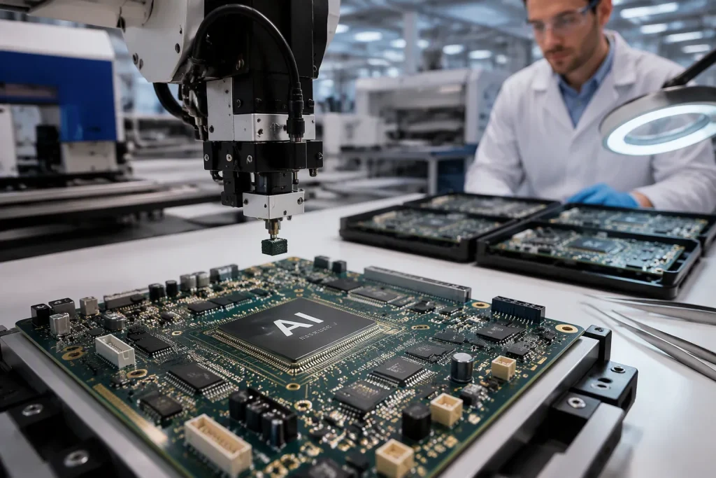
Enterprise IoT deployments are accelerating rapidly. Grand View Research projects the global enterprise IoT market will grow at a 14.1% compound annual growth rate from 2024 to 2030. This surge drives demand for intelligent gateways—devices that process data locally in smart buildings and industrial networks.
Bringing this hardware to market presents real hurdles. You must source specialized components, manage high-speed PCB layout risks, and coordinate multiple vendors. Traditional fragmented assembly models only amplify these delays.
A fast turnkey PCBA service offers a strategic alternative. This partnership consolidates your entire build—from BOM optimization to functional testing—under one roof. You gain a single partner for your AI gateway and enterprise IoT hardware.
This article explores the technical challenges of these devices, why a turnkey PCBA Singapore partner accelerates your timeline, and how quality-focused printed circuit board assembly reduces total cost. You will also learn how turnkey OEM PCBA scales from prototype to production.
Key Takeaways
A turnkey PCBA partner manages every step of your hardware build. This single point of contact reduces delays and errors.
Turnkey services include design reviews and component sourcing. These steps prevent costly mistakes and speed up production.
Quality is ensured through strict testing and standards. Your boards meet IPC Class 3 and pass functional tests.
Turnkey PCBA scales smoothly from prototype to production. You save time and money with a streamlined process.
A Singapore-based partner offers fast access to components. This location advantage accelerates your time-to-market.
AI Gateway PCBA Challenges in Enterprise IoT
Enterprise AI gateways combine multiple high-speed interfaces inside a compact enclosure. Your design must support multi-gigabit Ethernet, Power over Ethernet (PoE), PCIe, and DDR memory interfaces. These interfaces operate at high frequencies and require precise PCBA layout. Any signal integrity issue can cause data corruption or system failure. The fast project pace in the enterprise IoT market adds pressure. You need to move from prototype to production quickly without compromising quality.
High-Speed Design and Signal Integrity
High-speed signals travel on controlled impedance traces. Your PCBA must maintain consistent trace widths, layer stack-ups, and reference planes. A single mismatch creates reflections that degrade signal quality. For enterprise IoT gateways, this becomes critical. The device operates 24/7 in demanding environments. Signal integrity problems often surface only after deployment. A leading industry expert notes, “Signal integrity is the most common hidden defect in high-speed PCBA designs.”
Your turnkey PCBA partner must have experience with multi-layer boards. Six-layer or eight-layer PCBs are common for AI gateway designs. Each layer must be carefully planned to separate analog and digital signals. Ground planes must be continuous to reduce electromagnetic interference. The compact enclosure of a smart building gateway leaves little room for error. Every millimeter of the PCB layout must be optimized. Industry data shows that proper impedance control can reduce signal degradation substantially.
Thermal and Power Management for Edge Devices
Edge computing boxes generate significant heat. The processor, memory, and networking components all dissipate power. In a compact enclosure, airflow is limited. Heat builds up quickly and can damage components. Your PCBA must include thermal management features like thermal vias, heat sinks, or copper pours. Without these, the device may fail prematurely in the field.
Power management is equally important. PoE supplies power over the same cable as data. The voltage must be regulated efficiently. A poorly designed power circuit can cause voltage drops or noise. This noise couples into sensitive analog circuits and degrades performance. Your turnkey PCBA service should include thermal simulation and power integrity analysis. These steps prevent failures before mass production. IPC Class 3 standards apply to these high-reliability designs. Meeting these standards requires careful component selection and rigorous testing.
Turnkey PCBA Singapore: A Strategic Advantage
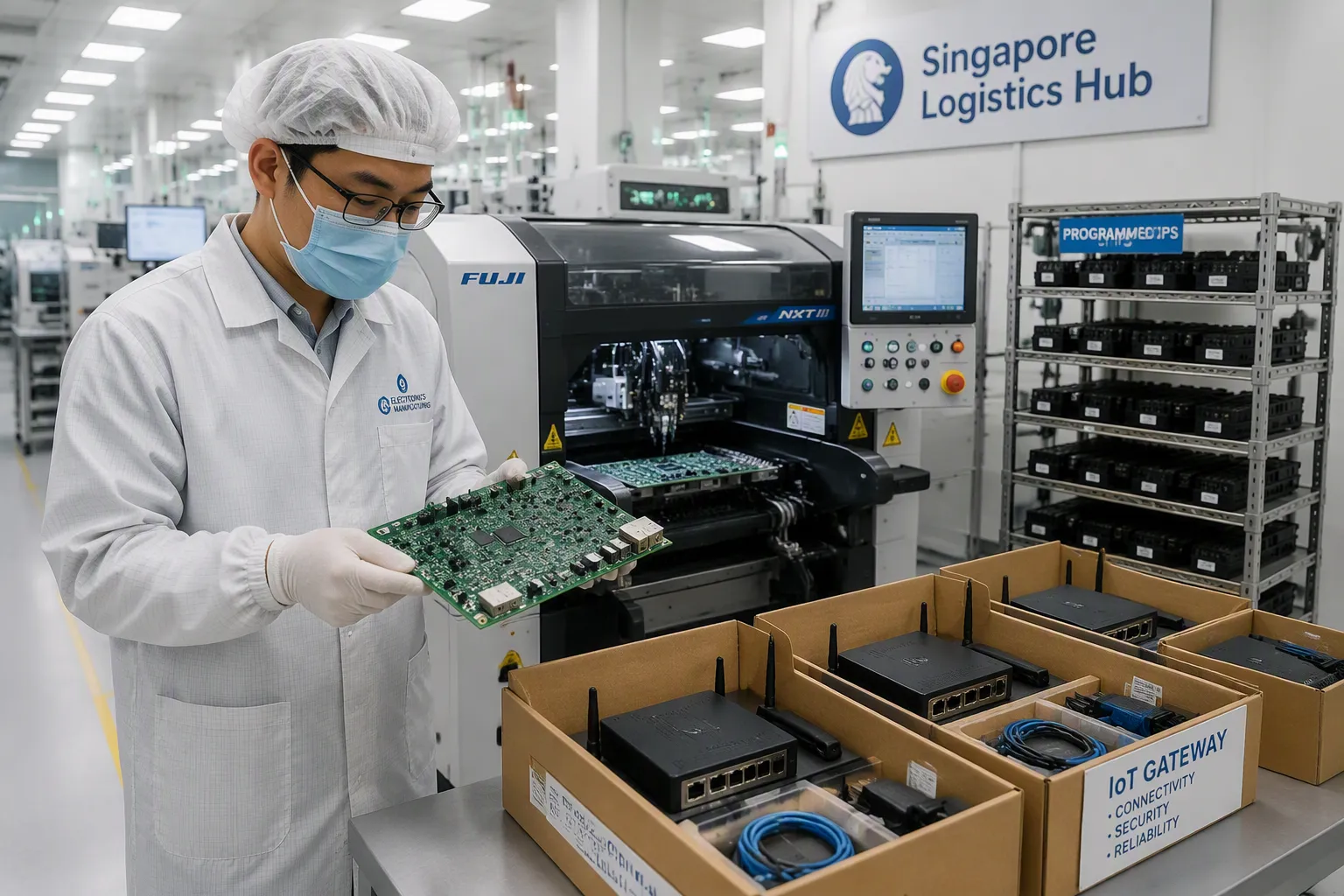
When you build AI gateways and enterprise IoT hardware, you face a complex web of vendors. Each vendor handles one piece of the puzzle. A PCB fabricator makes the board. An assembly house places components. A third party programs chips. A fourth company handles box build. This fragmented approach creates delays and miscommunication. A turnkey PCBA Singapore partner changes this equation entirely. You get one team that manages every step of the process. This single point of accountability reduces risk and speeds up your timeline.
One-Stop Lifecycle Management for IoT Hardware
A turnkey PCBA model gives you a single point of contact for your entire project. You work with one team from design review through final assembly. This simplifies communication and reduces errors. No more chasing multiple vendors for status updates. Your partner manages the full lifecycle from prototype to volume production.
Singapore plays a strategic role in this model. The city-state is a global logistics hub for electronics. Components arrive quickly from suppliers across Asia. You avoid the long lead times that plague other regions. A turnkey PCBA Singapore firm can source parts faster and consolidate shipments. This speed matters when you compete in the fast-moving enterprise IoT market.
The turnkey model also includes services you might not expect. Chip programming happens at the same facility as board assembly. Box build assembly – the final enclosure and wiring – is part of the same workflow. One vendor handles everything. This reduces your vendor management overhead significantly. You spend less time coordinating and more time designing.
Consider a real example. A company developing smart building gateways approached a turnkey PCBA partner. They needed 500 units with custom firmware and rigorous testing. The traditional approach would have required four separate vendors. The turnkey partner handled fabrication, assembly, chip programming, and box build in one workflow. The project completed in six weeks instead of twelve. The yield rate exceeded 98 percent. This is the power of a one-stop PCBA manufacturing approach.
A comparison shows the difference clearly. The table below contrasts the traditional model with a turnkey PCBA service.
Aspect | Traditional Assembly | Turnkey PCBA Service |
|---|---|---|
Points of contact | Multiple vendors | Single partner |
Typical lead time | 8-10 weeks | 4-6 weeks |
Yield rate | 92-95% | 98%+ |
Vendor management | High overhead | Minimal |
Proactive DFM and Component Sourcing
Design for Manufacturing (DFM) is a critical step in turnkey PCB assembly. Your partner reviews your layout before production begins. They check for signal integrity issues, thermal problems, and assembly challenges. This proactive approach prevents costly rework later. The review happens before you commit to tooling. This saves both time and money.
For AI gateway designs, DFM feedback is especially valuable. Your board has high-speed signals, dense components, and tight spacing. An experienced turnkey OEM PCBA partner knows where problems hide. They suggest adjustments to trace widths, via placement, or component orientation. These small changes make a big difference in yield.
Multi-layer boards for AI gateways require careful DFM analysis. The high layer count increases the risk of manufacturing defects. A turnkey partner reviews each layer for proper spacing and clearance. This reduces the chance of shorts or opens during assembly.
Industry data shows that DFM review can reduce assembly defects by up to 30 percent. The earlier you catch issues, the less they cost to fix. A turnkey partner integrates DFM into the standard workflow. You receive feedback before any production begins. This saves time and money.
Component sourcing is another area where the turnkey model excels. Specialized components for enterprise IoT gateways can be hard to find. A turnkey partner with strong supplier relationships can secure these parts faster. They also verify component authenticity and quality. This protects you from counterfeit parts that could cause failures in the field. The partner manages inventory and handles end-of-life issues for components. This keeps your supply chain running smoothly.
A turnkey OEM PCBA partner in Singapore leverages the region’s electronics ecosystem. They access a wide network of suppliers and distributors. This network ensures you get the right components at competitive prices. The result is a faster, more reliable path from design to production. You gain a strategic advantage in bringing your product to market quickly.
Ensuring Quality with Advanced Testing and Compliance
Enterprise IoT gateways operate around the clock in demanding environments. A failure in a smart building controller or industrial network device can disrupt operations for hundreds of users. This reality demands rigorous quality assurance throughout your PCBA manufacturing process. You need more than visual inspections and basic continuity checks. You need a comprehensive testing strategy that validates every solder joint, every connection, and every functional pathway on your board.
Adherence to IPC Class 3 and Industry Standards
IPC Class 3 represents the highest tier of quality and reliability in electronics manufacturing. This classification applies to critical applications where downtime is unacceptable. Your AI gateway hardware falls squarely into this category. The standard demands perfection in solder joint quality, with near-zero tolerance for defects.
The acceptance criteria for Class 3 boards are precise. Solder joints must achieve 100% side joint fillet coverage on surface mount components. Through-hole connections require a minimum 75% circumferential fillet. Ball grid array voids must not exceed 9% of the joint area. Component placement tolerance tightens to ±0.1 mm. Ionic contamination limits stay below 0.78 μg NaCl/cm². These measurements demand fractions of a millimeter in precision.
Criterion | Class 3 Requirement |
|---|---|
Solder Joint Wetting (Surface Mount) | 100% side joint fillet required |
Through-Hole Fillet | Minimum 75% circumferential fillet |
BGA Void Content | Must not exceed 9% |
Component Placement Tolerance | ±0.1 mm |
Ionic Contamination Limit | ≤ 0.78 μg NaCl/cm² |
Minimum Heel Fillet | 25% of lead width |
A turnkey PCBA partner with Class 3 capabilities maintains strict process controls. They calibrate reflow ovens precisely. They verify solder paste thickness on every board. They conduct 100% X-ray inspection on high-reliability boards. This level of scrutiny yields measurable results. High-reliability assemblies that undergo complete X-ray inspection achieve defect rates below 300 parts per million for solder joints.
The source guarantees a defect rate of less than 300 parts per million (ppm) for solder joints, specifically for high-reliability boards that undergo 100% X-ray inspection.
Bonysn’s Singapore facility follows these exacting standards. Every board receives the same attention regardless of order size. You gain confidence knowing your enterprise IoT hardware meets the strictest industry benchmarks.
Functional Testing and Traceability Protocols
Visual inspection and X-ray analysis confirm solder joint quality. However, they cannot verify that your board actually works. Functional testing bridges this gap. Your PCBA partner should perform in-circuit testing (ICT) to check each component’s electrical performance. Boundary scan testing validates connections between digital components. Final functional tests simulate real operating conditions to confirm the board performs as designed.
For AI gateway boards, functional testing takes on added importance. The board must handle high-speed data transmission, power management, and network connectivity simultaneously. A functional test rig replicates these conditions. It checks Ethernet links, PoE power delivery, and processor boot sequences. Any anomaly triggers immediate investigation.
Traceability completes the quality picture. Every component on your board carries a unique identifier. Your PCBA partner records which batch of components went into each board. They track solder profiles, inspection results, and test outcomes. This data becomes invaluable for after-sales support. If a field failure occurs, you can trace the exact production run and identify potential causes quickly.
Singapore’s electronics industry has embraced these rigorous protocols. The city-state’s position as a regional quality hub means local manufacturers invest heavily in test infrastructure. A turnkey PCBA Singapore partner offers this depth of capability. You receive boards that meet Class 3 standards, pass comprehensive functional tests, and carry complete traceability records. This combination ensures your enterprise IoT hardware performs reliably for years.
Scaling from Prototype to Production with Turnkey OEM PCBA
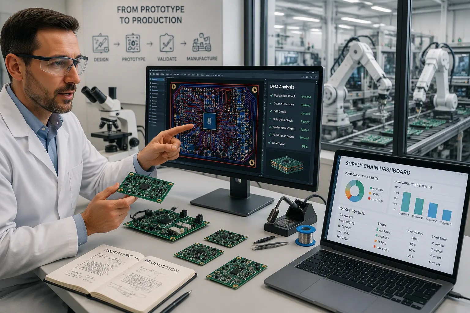
The journey from prototype to volume production often determines your product’s success. Many companies struggle at this transition. They design a working prototype, then face unexpected challenges during mass production. Component shortages appear. Assembly defects emerge. Yields drop. Your timeline slips. A turnkey OEM PCBA partnership eliminates these surprises through structured scaling.
Accelerating Time-to-Market with Rapid Prototyping
Rapid prototyping accelerates your development cycle. Your turnkey PCBA partner builds small batches quickly, often within days. You receive functional boards for validation. You test them in real-world conditions. You gather performance data. This feedback loop drives design improvements before you commit to expensive tooling.
DFM feedback during this phase prevents costly rework later. Your PCBA partner reviews each prototype against manufacturing constraints. They identify potential solder joint issues. They flag component placement problems. They suggest trace width adjustments for better signal integrity. These recommendations arrive before mass production begins. You implement changes while the design remains flexible. Rework costs at this stage stay minimal.
Consider the economics. A design error discovered during prototyping costs hundreds of dollars to fix. The same error found during mass production costs thousands. You might need to scrap entire batches of boards. You might face delays of weeks while new boards arrive. The earlier you catch issues, the less they cost. Industry data shows that DFM review reduces assembly defects by up to 30 percent. Each PCBA iteration brings you closer to a production-ready design.
Your turnkey pcb assembly partner also accelerates prototyping through component availability. They maintain relationships with suppliers across Asia. They source parts quickly for your small batch. You avoid the long lead times that delay many prototype cycles. Singapore’s position as a logistics hub amplifies this advantage. Components move through the region rapidly. Your prototype boards arrive faster.
Cost Reduction Through Supply Chain Consolidation
Consolidated purchasing power delivers measurable cost savings. Your turnkey oem pcba partner buys components for many clients. This volume commands better pricing from suppliers. You benefit from these economies of scale. Your unit costs drop compared to purchasing components independently.
The savings extend beyond component pricing. You eliminate multiple vendor contracts. You reduce administrative overhead. You avoid shipping costs between separate facilities. Your PCBA partner manages inventory, so you avoid holding excess stock. Each of these factors contributes to a lower total cost of ownership.
Cost Factor | Traditional Model | Turnkey OEM PCBA |
|---|---|---|
Component pricing | Retail or small-volume | Volume-discounted |
Vendor management | Multiple contracts | Single agreement |
Logistics | Multiple shipments | Consolidated |
Rework costs | Higher defect rates | DFM-driven reduction |
Typical lead time | 8-10 weeks | 4-6 weeks |
A turnkey pcba singapore partner offers additional advantages. Singapore’s electronics ecosystem provides access to a wide supplier network. Your partner leverages these relationships to secure favorable terms. They also manage component lifecycle issues. When a part approaches end-of-life, they source alternatives proactively. This protects your production schedule from unexpected disruptions.
The strategic benefit extends to future product generations. Your turnkey partner learns your design patterns. They understand your quality requirements. They anticipate your component needs. This institutional knowledge accelerates each subsequent product launch. You build a scalable partnership that grows with your business. Your ai gateway products reach market faster with each iteration. Your enterprise IoT hardware maintains consistent quality across generations.
The table above shows the cost comparison clearly. Traditional models carry hidden expenses. Turnkey models consolidate these costs into a single, predictable structure. You gain clarity on your true production costs. You make better business decisions with this visibility.
A scalable partnership means each new product generation benefits from accumulated knowledge. Your PCBA partner already understands your design philosophy, quality standards, and component preferences. This continuity compounds your competitive advantage.
AI gateways and enterprise IoT hardware demand precision at every stage. You need a partner who understands high-speed signal integrity, thermal constraints, and IPC Class 3 compliance. A fast turnkey PCBA service in Singapore delivers exactly that expertise.
This model consolidates your printed circuit board assembly under one roof. You overcome supply chain hurdles, reduce total cost of ownership, and accelerate your timeline. The turnkey oem pcba approach transforms complex builds into manageable workflows.
Your next step is clear. Contact our team to discuss your specific project, request a DFM review, or obtain a quote. Turn your design into a deployable product with a pcb assembly service built for speed and reliability.
FAQ
How quickly can you provide a quotation for my AI gateway project?
You receive a detailed quotation within 48 hours of submitting your BOM and Gerber files. The quote includes component costs, assembly fees, and testing charges. This rapid turnaround lets you evaluate your budget without delay. Most clients receive their complete quote within two business days.
How do you handle component sourcing for hard-to-find parts?
Your Singapore-based partner maintains strong relationships with suppliers across Asia. This network secures specialized components quickly. You avoid long lead times and counterfeit risks. The team verifies every part’s authenticity before assembly begins. This proactive approach keeps your production schedule on track.
What does your DFM review process include?
Our engineers analyze your layout for signal integrity, thermal management, and assembly challenges. You receive a detailed report with actionable recommendations before production starts. This review catches potential defects early. Industry data shows this process reduces assembly defects by up to 30 percent. Your pcba design improves before you commit to tooling.
What quality certifications does your Singapore facility hold?
Your boards meet IPC Class 3 standards, the highest reliability tier for electronics manufacturing. The facility performs 100% X-ray inspection on high-reliability boards. Solder joint defect rates stay below 300 parts per million. Every pcba unit carries complete traceability records for after-sales support.
See Also
Ready To Use AI Gateway PCBA For Singapore IoT MedTech
Complete AI PCBA Service For Singapore IoT And MedTech Projects
All Inclusive AI PCBA For Irish MedTech IoT Hardware Firms