
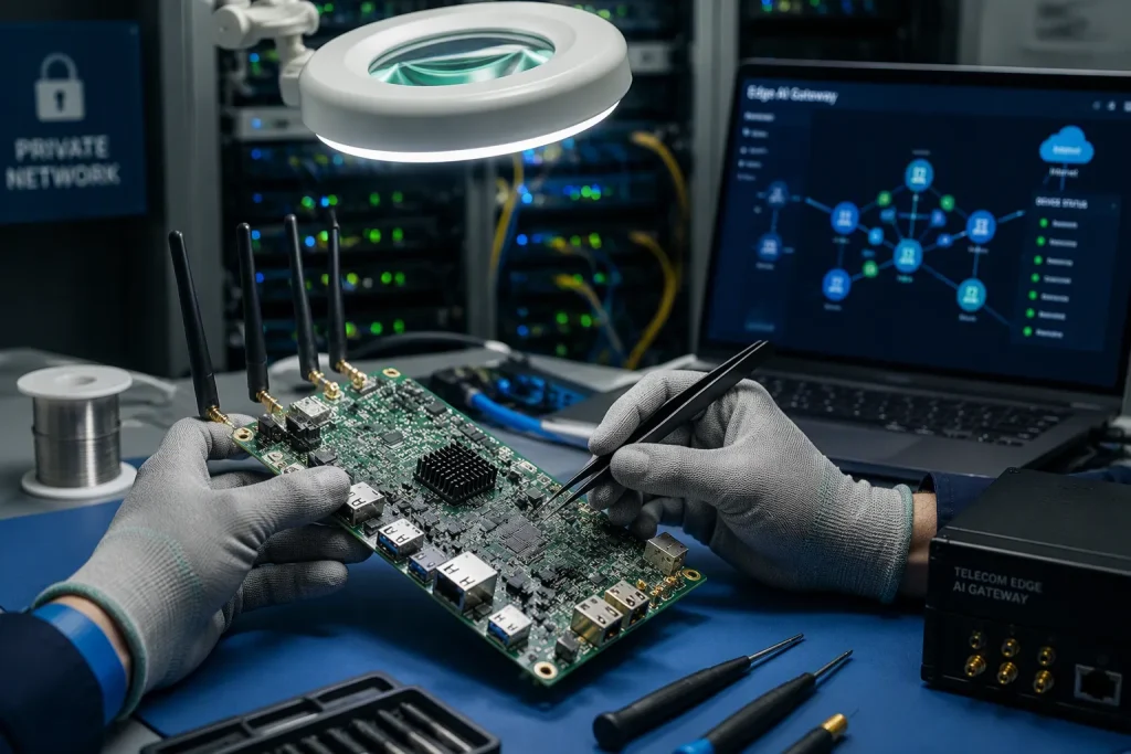
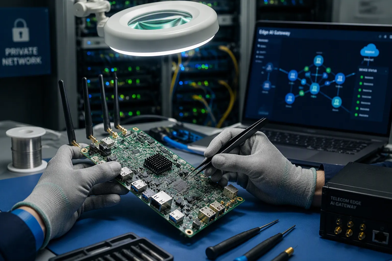
Telecom edge AI PCBA transforms private 5G gateway and industrial router designs. This technology enables on-device AI inference at the network edge. Engineers now select higher-performance processors, denser layouts, and advanced thermal solutions. Assembly processes demand greater rigor.
This shift reshapes component selection, signal integrity, power delivery, and manufacturing. Designers of gateways, industrial routers, edge inference devices, and communication monitors face new constraints. PCBA design for 5G and telecommunication equipment must balance performance with reliability.
Edge computing and 5G technology drive these changes. PCBs and PCBA assemblies for 5G networks require careful planning. This article guides engineers and technical managers who make decisions for private network deployments.
Key Takeaways
Edge AI PCBA design requires advanced processors, denser layouts, and better thermal solutions for private 5G networks.
Industrial routers need rugged protection and efficient heat dissipation to handle harsh environments and AI workloads.
Dense edge AI boards make soldering and testing harder, so engineers must use precise processes and rigorous validation.
Edge AI reduces latency and backhaul traffic, but increases cost and complexity in hardware and assembly.
Best practices like design-for-manufacturing and thermal co-design help engineers build reliable PCBs for private networks.
Telecom Edge AI PCBA Impact on 5G Gateway Design
Processor, Memory, and Stackup Shifts
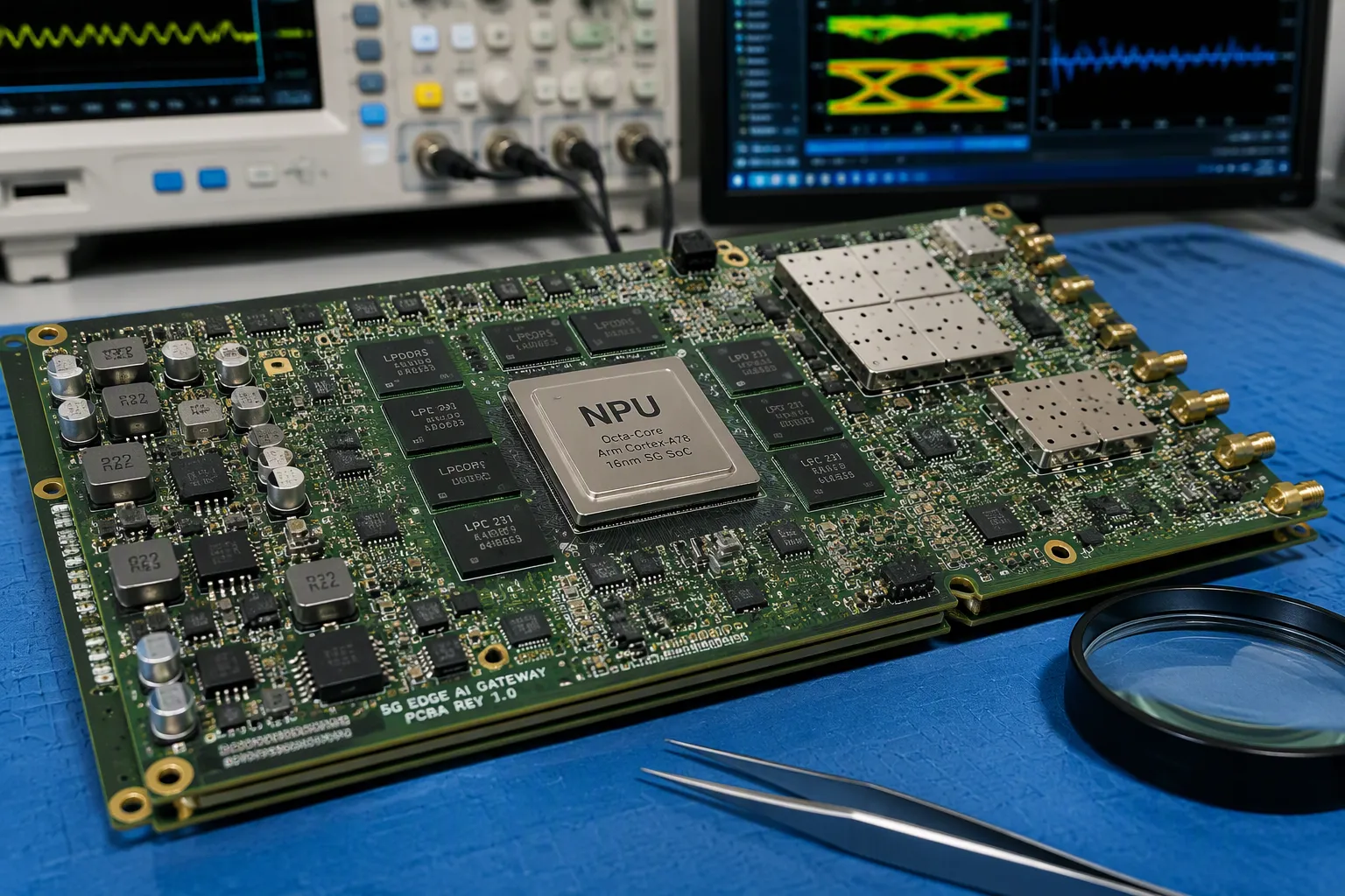
Edge AI inference near the data source forces engineers to rethink every layer of the board. A telecom edge ai pcba now carries application processors with integrated neural processing units, high-speed memory, and high-speed data lanes. These components demand denser interconnect and more complex layer stacks than earlier gateway designs.
A typical stackup increases, with added layers to separate high-speed digital routing from analog and RF sections. This separation protects 5g technology on pcba design and functionality. Designers also place ground planes between sensitive traces to reduce crosstalk.
Memory placement matters equally. Engineers route memory traces with matched lengths and controlled impedance. These 5g pcba designs must handle data rates that push beyond previous generation limits. The processor-to-memory channel becomes a critical path for both performance and signal integrity.
Power Delivery and RF Signal Integrity
Power delivery networks for edge AI gateways must supply multiple voltage rails with tight regulation. A typical board supports core voltages for the processor, I/O rails, memory rails, and RF front-end supplies. Each rail requires dedicated regulator phases and bulk decoupling.
High-frequency signal integrity depends on careful power integrity. Noise on the power plane couples directly into RF paths. Engineers use low-dropout regulators with high power supply rejection ratio near sensitive analog circuits. They also place ferrite beads and pi filters to isolate digital switching noise.
The 5g technology on pcba design for these gateways combines secure, high-bandwidth connectivity with on-board AI computation. This dual requirement creates tension between thermal density and RF performance. Heat generated by AI accelerators can shift RF component values. Designers address this through thermal vias, copper pours, and strategic component placement.
Firmware integration adds another layer of complexity. Engineers must coordinate boot sequences, sensor interfaces, and power management states across multiple processors. Enclosure fitting constrains board dimensions and connector placement. Product certification for 5g networks demands rigorous EMI/EMC shielding and antenna design and optimization.
The pcba’s critical role in 5g and telecommunication equipment becomes clear when considering these constraints. Key design considerations for 5g pcba include thermal management, power sequencing, and RF isolation. Shielding and grounding techniques protect high-frequency rf signals from interference. Controlled impedance routing ensures reliable data transmission across all interfaces.
Engineers who master these elements deliver gateways that perform reliably in private network deployments. The 5g pcba functionality and performance depends on getting every detail right, from stackup selection to final assembly.
5G Technology on PCBA Design for Industrial Routers
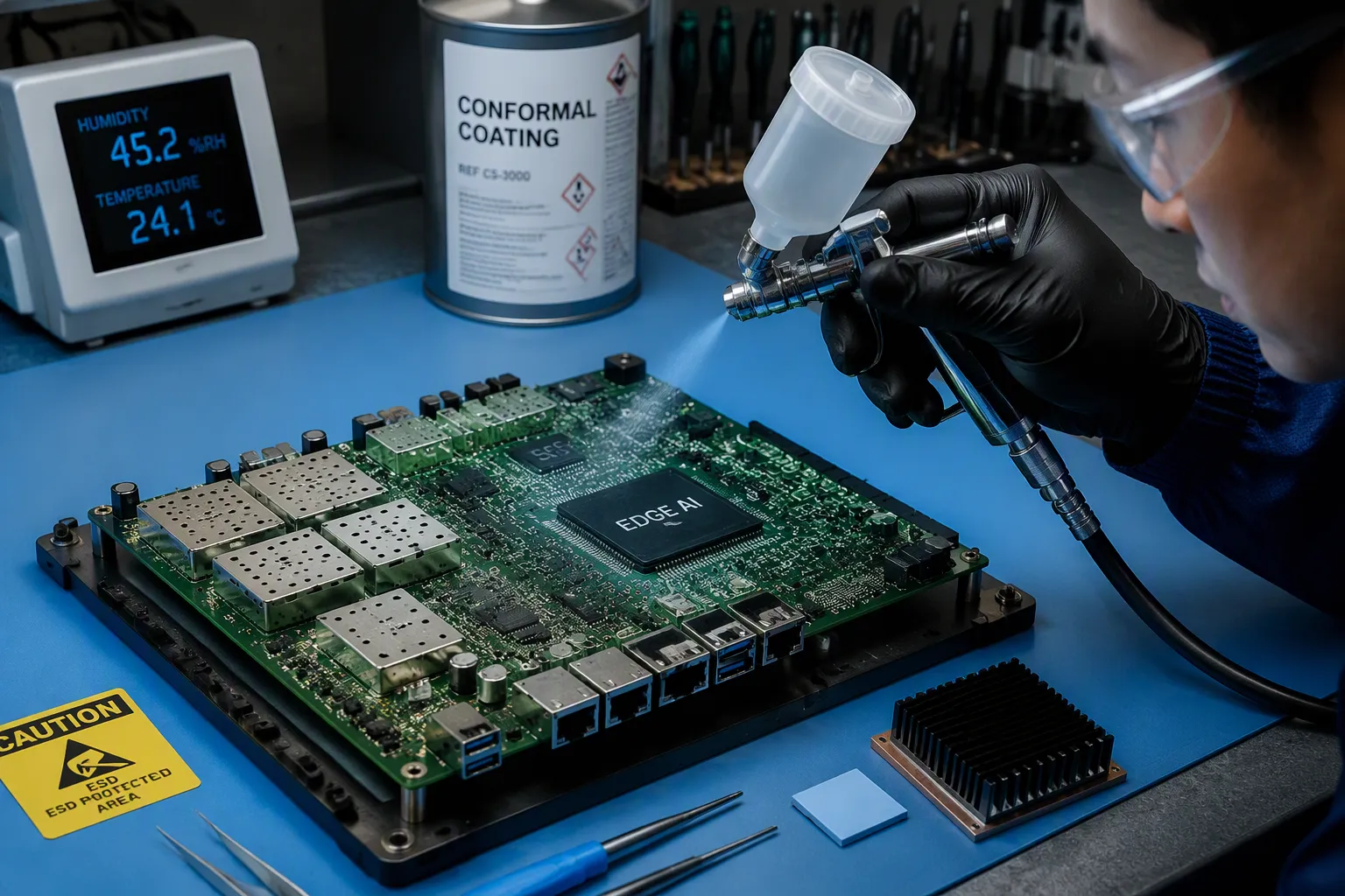
Telecommunication PCBA for industrial routers differs from general circuit boards in fundamental ways. These boards must support high-frequency signal transmission. They fit into compact form factors. They operate reliably in demanding environments with temperature extremes, vibration, and humidity. Edge AI boards in private infrastructure add further complexity. They require optimized thermal design and power delivery to sustain AI workloads while meeting low latency and high reliability demands of industrial automation.
Ruggedization and Thermal Management
Telecom edge ai pcba requires specialized protection against harsh operating conditions. Conformal coating provides a critical defense layer for these boards used in damp, humid, or dusty environments.
For PCBs that will be used in damp, humid, hot, dusty, or other harsh environments, a special process known as conformal coating is often required. Through this process, the assembled PCB is covered in a thin layer of non-conductive, protective material such as Silicon, Acrylic, Urethane, or Paraxylene. Once cured, it increases the overall durability of the product while also protecting it from outside contaminants.
Several coating types suit different environmental challenges:
Acrylic: good moisture resistance for moderate environments; easy to apply and rework.
Silicone: highly flexible and heat-resistant up to 200°C.
Polyurethane: excellent chemical resistance for harsh industrial settings.
Parylene: superior protection via vapor deposition but harder to apply and remove.
Coating thickness ranges from 25 to 75 micrometers. For high-humidity areas, engineers apply a thicker coating closer to 75 micrometers for better insulation. Clean the board thoroughly before coating to remove flux residue that can trap moisture.
Thermal management presents an equally significant challenge. Edge AI processors generate substantial heat within fanless enclosures. Engineers use simulation tools to validate heat dissipation. The table below summarizes common methods:
Method/Tool | Description |
|---|---|
Steady-state FEM simulation | ANSYS Icepak used to validate thermal performance of fanless enclosures. |
IR thermography | Validates lateral temperature gradient ≤2°C under 30W load. |
Contact resistance measurement | Measured per ASTM D5470, required <5 mm²·K/W to ensure proper heat transfer. |
AI-assisted thermal simulation employs machine learning to predict thermal energy flow through a device during real-world usage. This method enables rapid design iteration in the prototyping phase. It gives confidence that fanless edge AI units will not overheat in the field. The pcba’s critical role in 5g and telecommunication equipment becomes evident when considering these constraints. Proper heat dissipation directly impacts 5g technology performance and long-term reliability.
Real-Time Processing and Interface Changes
Industrial automation demands real-time processing with deterministic latency. 5g technology on pcba design and functionality must support low response times. Engineers select processors with hardware acceleration for AI inference. They redesign memory interfaces and data paths to minimize delay.
The shift to edge AI changes the interface layout on 5g pcba designs. Traditional gateways use separate modules for processing and radio functions. New designs integrate these elements on a single board. This integration reduces latency but increases design complexity.
Power delivery must support sustained AI workloads without thermal buildup. Engineers use multiple voltage rails with tight regulation. They place decoupling capacitors close to processor power pins. They design the stackup to minimize inductance in power paths.
Board design for industrial gateways also requires careful attention to signal integrity. High-speed SerDes lanes carry data between processors and radio modules. Controlled impedance routing preserves signal quality. Ground planes shield sensitive traces from interference. Designers test these pcbas for compliance with strict telecommunication standards.
5g technology continues to shape requirements for industrial applications. The combination of ruggedization, thermal control, and real-time processing defines modern industrial designs. Engineers who master these elements deliver reliable products for private networks.
PCBA Design and Assembly Considerations
Soldering Challenges and Material Choices
Dense edge AI boards push soldering processes to their limits. Fine-pitch components, micro BGAs, and ultra-small passives leave little room for error. Solder paste deposition must be precise. Reflow profiles must account for varied thermal masses across the board. A large processor heats differently than a small RF filter. Engineers must profile each zone carefully.
Material choices matter for long-term reliability. High-temperature solder alloys suit boards that operate continuously at elevated temperatures. The pcba design must specify materials that resist thermal fatigue. For 5g and telecommunication equipment, lead-free alloys with enhanced thermal cycling performance are common. Underfill protects BGA joints from stress. Conformal coating adds environmental protection.
Bonysn supports multi-layer high-speed PCB fabrication and BGA assembly. Their experience with communication interface assembly helps customers overcome challenges in manufacturing 5g pcbas. The table below compares assembly approaches:
Feature | Standard Assembly | Bonysn Advanced Assembly |
|---|---|---|
Layer count | Standard | High |
BGA pitch | Standard | Fine |
Thermal vias | Basic | Optimized |
Testing for High-Speed and RF Performance
Testing validates high-frequency signal integrity and overall reliability. Engineers use time-domain reflectometry to check impedance. Vector network analyzers measure S-parameters. These tests confirm that 5g pcba designs meet performance targets. The pcba’s critical role in 5g and telecommunication equipment demands rigorous validation.
High-temperature continuous operation testing reveals weaknesses. Boards run at elevated temperatures for extended periods. Engineers monitor signal degradation and component drift. This testing supports antenna design and optimization for 5g technology. It also verifies 5g technology on pcba design margins. Bonysn cooperates on thermal design to help customers pass these tests. Their testing aligns with IPC standards.
Benefits and Trade-Offs of Edge AI Integration
Latency Reduction and Bandwidth Optimization
Edge AI integration delivers its most visible gain in latency. Inference happens on the gateway itself, so data does not travel to a distant cloud server and back. Industrial automation demands low response times, and local processing makes that target achievable. A 5g private network already offers fast wireless links. Edge AI removes the remaining delay from the backhaul path.
Bandwidth savings follow naturally. A communication monitor that filters and classifies data locally sends only relevant events upstream. This approach reduces backhaul traffic and eases congestion on shared links. Engineers who design low-latency, reliable pcba connections enable this architecture at the hardware level. Controlled impedance routing and proper shielding keep the data path clean from antenna to processor.
Cost, Complexity, and Scalability
The trade-offs deserve equal attention. Edge AI hardware costs more than a conventional gateway board. Higher-performance processors, denser stackups, and advanced thermal solutions raise both material and assembly expenses. A 5g deployment with many nodes multiplies that cost across the network.
Complexity grows in parallel. Designers must manage power sequencing, thermal margins, and RF isolation on a single board. Testing requirements expand to cover high-speed and RF performance together. Scaling a proven pcba design across many units helps amortize these costs. Modular approaches let engineers reuse validated blocks for new 5g technology variants. Teams that invest early in design-for-manufacturing and rigorous validation reduce per-unit cost over time. The pcbas in a mature product line benefit from shared tooling and established process windows. This strategy keeps 5g edge deployments economically viable as network size grows.
Best Practices for Edge AI PCBA Implementation
A disciplined pcba design approach starts with design-for-manufacturing and design-for-test strategies. Telecom edge ai pcba boards combine dense digital logic with high-frequency RF sections. An assembly defect on such boards can cause expensive rework or field failure.
Design-for-Manufacturing and Design-for-Test
DFM begins with component placement. Designers leave sufficient clearance around large BGAs for underfill dispensing. They orient similar components in the same direction to simplify pick-and-place. Panelization includes tooling holes and fiducial marks for precise solder paste deposition. For boards with many layers, controlled impedance depends on consistent dielectric thickness. Engineers select materials with tight tolerance on dielectric constant and loss tangent for each pcba. These choices directly affect yield for 5g and telecommunication equipment.
DFT requires accessible test points for every critical node. Boundary scan tests interconnects on high-density BGAs where physical probing is impossible. Flying probe testing validates power rails and RF path continuity on each pcba. Vector network analysis confirms S-parameter targets for antenna feed lines. The integration of AI for production optimization now appears in state-of-the-art assembly lines. Machine learning algorithms analyze solder paste inspection data to adjust stencil parameters in real time. This approach reduces defect rates and improves first-pass yield for complex pcbas.
Thermal and Power Integrity Co-Design
Thermal management and power integrity must proceed together for edge AI boards. High-current rails serving AI processors generate heat that degrades power delivery efficiency. Engineers use electro-thermal simulation to model both domains simultaneously. They place voltage regulators close to processor power pins to minimize IR drop. Decoupling capacitors form a low-impedance path across a wide frequency range. Ground planes and thermal via arrays conduct heat away from hot components. Designers allocate inner copper layers as heat spreaders. They connect these layers to the enclosure through thermal interface materials. Co-design reduces design cycles and prevents late-stage fixes for each pcba.
These practices sustain AI workloads in private 5g gateways and industrial routers. Engineers confirm that junction temperatures stay below component ratings under worst-case conditions. They verify power plane impedance meets targets across all operating frequencies. For 5g pcba designs carrying edge AI processors, this methodology is essential. The 5g technology embedded in these boards demands rigorous validation. Engineers who follow these best practices deliver reliable products for private network deployments.
Telecom edge ai pcba reshapes private 5g gateway and industrial router. Designers specify higher-performance processors, denser layouts, and advanced thermal solutions. Assembly and testing processes demand greater sophistication than conventional designs.
Edge AI delivers lower latency and reduced backhaul dependency. It enables enhanced on-device intelligence at the network edge. Private 5g networks benefit from real-time processing capability. These advantages come with trade-offs in cost and complexity.
Engineers should adopt design-for-manufacturing and thermal co-design best practices. Rigorous testing ensures reliable deployment for private networks. The pcba design must balance these competing demands.
Future edge AI hardware trends will continue to shape design requirements. The pcbas of tomorrow will demand higher density and thermal performance.
FAQ
What makes telecom edge AI PCBA different from a standard gateway board?
Edge AI boards carry neural processing units, high-speed memory, and high-speed data lanes. These parts demand denser stackups, tighter impedance control, and stronger thermal paths. A standard gateway board cannot support on-device inference at the network edge.
How does 5g technology change industrial router assembly?
Industrial routers need high-frequency transmission, compact form factors, and reliable operation in harsh environments. Assembly must handle fine-pitch components and controlled impedance routing. Conformal coating and thermal management protect the board in the field.
Why do dense edge AI boards challenge soldering and testing?
Micro BGAs and ultra-small passives leave little process margin. Reflow profiles must match varied thermal masses across the board. Testing combines time-domain reflectometry, vector network analysis, and high-temperature continuous operation runs to confirm performance.
How does Bonysn support complex pcbas for private networks?
Bonysn builds multi-layer high-speed boards and handles BGA assembly for communication interfaces. Their process supports high layer count and fine BGA pitch with optimized thermal vias. Testing aligns with IPC standards.
What trade-offs should engineers expect from edge AI integration?
Edge AI cuts latency and backhaul traffic, but raises material and assembly cost. Complexity grows across power sequencing, thermal margins, and RF isolation. Modular designs and early design-for-manufacturing work reduce per-unit cost as networks scale.
See Also
Reliable PCB Assembly For UK Edge AI Inference Servers
Bespoke Edge AI Circuit Board Assembly For US Hardware Startups
Full-Service AI Gateway PCBA For Singapore IoT And MedTech
All-Inclusive AI Server PCB Assembly Service For Singapore Data Centers
Integrated AI Server Board Assembly For Singapore Data Centers