
Custom edge AI PCBA revolutionizes how you approach hardware development. This technology enhances design efficiency, allowing you to streamline processes and reduce time-to-market. With cost-effective solutions, you can allocate resources more effectively, driving innovation. Real-world applications, from robotics to smart cameras, demonstrate the capabilities of custom edge AI PCBA, empowering your startup to create cutting-edge products that meet market demands.
Key Takeaways
Custom edge AI PCBA boosts design efficiency by allowing concurrent design, simulation, and prototyping, leading to faster product delivery.
Cost savings arise from optimized designs and streamlined assembly processes, reducing overall manufacturing expenses and improving unit economics.
AI applications in robotics and smart cameras enhance local data processing, improving response times and reliability in various environments.
Transitioning from prototypes to production requires careful validation, supply chain setup, and continuous monitoring to ensure quality and scalability.
Embracing custom edge AI PCBA positions startups to innovate rapidly and stay competitive in a growing market projected to reach $154 billion by 2030.
Benefits of Custom Edge AI PCBA
Design Efficiency
Custom edge AI PCBA significantly enhances design efficiency in hardware development. By leveraging AI-assisted circuit board design, you can streamline your design processes. This technology allows for concurrent design, simulation, and prototyping, which accelerates product delivery without compromising quality.
Here are some key methodologies that improve design efficiency:
Concurrent design, simulation, and prototyping: This approach shortens the time from concept to market.
Structured feasibility assessments: These assessments help you make quicker decisions, preparing your platforms for rapid prototyping and deployment.
Full-cycle process: This ensures your hardware is functional, field-ready, and engineered for performance.
AI technologies also automate complex tasks, such as layout optimization and error checking. For instance, AI-driven PCB design tools analyze schematics and propose optimal component layouts. This reduces manual rework, allowing you to focus on higher-level challenges. Real-time Design Rule Checking (DRC) surfaces errors during the design process, preventing costly revisions and speeding up production.
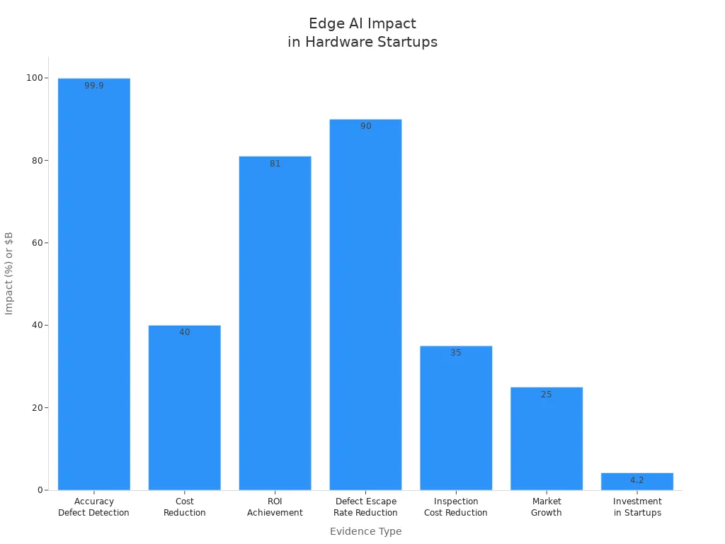
The impact of these methodologies on design efficiency is substantial. A recent study showed that companies utilizing custom edge AI PCBA experienced a 30% reduction in design cycle time. This efficiency translates into faster time-to-market, giving you a competitive edge.
Cost Savings
Cost savings are another significant advantage of custom edge AI PCBA. By optimizing designs for automation and including designated test points, you can streamline the assembly process. This reduces overall assembly time and operational expenses.
Consider the following advantages of custom edge AI PCBA compared to traditional solutions:
Advantage | Description |
|---|---|
Faster Time-to-Market | Bypasses separate procurement and assembly stages, allowing quicker transition from design to testing. |
Improved Quality and Reliability | Utilizes automated processes to ensure precision, reducing risks of defects. |
Streamlined Supply Chain Management | A single vendor manages the entire process, simplifying logistics and reducing costs. |
Cost Efficiency in the Long Run | Minimizes rework and waste, leading to lower overall project costs. |
Enhanced Design Flexibility | Full control over PCB layout, components, and features tailored to specific needs. |
Comprehensive Testing and QA | Multi-stage testing ensures only functional boards are delivered. |
Scalability and Production Efficiency | Ability to transition smoothly from prototypes to mass production without quality compromise. |
Successful implementations of custom edge AI PCBA illustrate these benefits. For example, OLogic developed sophisticated electronics for tractors that make real-time decisions on identifying weeds. This innovation not only improved efficiency but also reduced operational costs for farmers. Similarly, Snorble created an AI-powered companion for children that processes interactions locally, ensuring data privacy while minimizing costs associated with cloud storage.
By adopting custom edge AI PCBA, you can significantly reduce manufacturing costs. As production scales, automation enhances efficiency, and sourcing components becomes more cost-effective. This leads to reduced costs per unit and improved consistency.
AI Applications in Edge Devices

Robotics and Automation
AI applications running at the edge have transformed robotics and automation, enabling devices to process data locally. This capability enhances reaction times and reliability, especially in environments with limited connectivity. You can leverage edge AI to create autonomous systems that perform complex tasks efficiently.
Consider the following applications of edge AI in robotics:
Autonomous Mobile Robots (AMRs): These robots navigate and operate independently, making real-time decisions based on sensor data.
Smart Factory Automation: AI-driven inspection technology optimizes production lines, ensuring quality control without human intervention.
Multi-Camera Inspection Systems: These systems utilize AI for real-time analysis, detecting defects with high accuracy.
AI-Powered Security Platforms: Robots equipped with edge AI can monitor environments and respond to threats instantly.
Warehouse Robotics: Automated systems streamline logistics, improving efficiency and reducing operational costs.
Agricultural Robotics: AI applications enhance precision farming, allowing for targeted interventions based on real-time data.
Smart City Infrastructure: Edge AI supports traffic management and public safety initiatives, improving urban living conditions.
Advanced Machine Vision Solutions: These solutions enable robots to interpret visual data, enhancing their operational capabilities.
The integration of custom edge AI PCBA in these applications allows for tailored designs that meet specific operational needs. For instance, custom PCBA can optimize signal integrity analysis and power integrity evaluation, ensuring that robots function effectively in diverse environments.
Performance Improvement | Description |
|---|---|
Tailored to Specific Functions | Custom PCBA can be designed for specific tasks, enhancing real-time response and fail-safe features. |
Space and Weight Optimization | Custom designs help reduce weight and size, crucial for applications like drones. |
Custom Connectivity Options | Allows selection of specific connectivity technologies, improving system efficiency. |
Easier Integration and Upgrades | Custom protocols facilitate easier integration and future upgrades, reducing maintenance costs. |
Smart Edge Cameras
Smart edge cameras represent a significant advancement in surveillance and monitoring technology. These devices process data on-site, which minimizes latency and enhances privacy. By utilizing custom edge AI PCBA, you can develop cameras that deliver superior performance compared to traditional systems.
Key features of smart edge cameras include:
Feature | Description |
|---|---|
Image Sensor | 5MP low noise onsemi® AR0521 CMOS Image Sensor |
Processor | Powerful dual-core processor |
AI Capabilities | Advanced AI capabilities for real-time analysis |
Framework Support | Support for frameworks like TensorFlow Lite Micro and DeepviewRT |
ISP | On-board high-performance ISP for auto-exposure and auto-white balance |
Smart edge cameras excel in various applications, including security surveillance, traffic monitoring, and industrial inspection. They provide faster and more reliable quality control by processing data locally, which reduces bandwidth usage and enhances security.
Feature | Smart Edge Cameras | Traditional Camera Systems |
|---|---|---|
Data Processing Location | Local (on-device) | Remote (cloud-based) |
Latency | Minimal, enabling real-time decisions | Higher, due to data upload delays |
Bandwidth Usage | Reduced, as data is processed locally | High, requires streaming large data |
Privacy and Security | Enhanced, data remains on-site | Vulnerable, data processed off-site |
Speed of Insights | Instant, due to local processing | Slower, reliant on cloud processing |
The integration of Jetson boards in smart edge cameras enhances their functionality. Jetson technology supports advanced AI applications, enabling real-time data processing and analytics. This modular design allows for reliable edge AI solutions, essential for security and analytics.
By adopting these technologies, you can create innovative solutions that meet the demands of modern applications. The growth of edge AI in manufacturing and robotics is evident, with a market projected to reach $15.7 billion by 2027.
Transitioning from Prototypes to Production
From Gerber to PCB Manufacturing
Transitioning from prototypes to production involves several critical steps. First, you must finalize your design. Lock in your design after thorough prototyping and testing. Use Design for Manufacturability (DFM) checklists to confirm manufacturability. Next, validate your design with small batches. Producing a small pre-production run, typically between 100 to 500 units, helps identify issues before full-scale manufacturing.
After validating your design, set up your supply chain. Secure components and materials for the full production volume, accounting for lead times of 4 to 12 weeks for specialized parts. Once your supply chain is in place, scale manufacturing. Partner with a manufacturer to ramp up production, starting with a pilot run to fine-tune processes. Finally, continuously monitor and optimize production. Keep an eye on quality metrics and production efficiency, adjusting processes as needed to maintain high standards.
Tip: A single defect during the pilot stage can cost 3 to 8 times more to fix than addressing it before production.
Scaling Production Volumes
Scaling production volumes effectively is crucial for hardware startups. You need to adopt smart design optimization strategies. AI algorithms can predict optimal PCB layout and component placement, enhancing performance. Intelligent testing and quality assurance (QA) measures are essential. Automated AI testing can detect defects that human inspectors might miss, ensuring quality.
As you scale, consider the structural costs that arise from increased volume. A significant jump in production can lead to complications that were manageable at lower volumes. Address these challenges proactively to ensure a smooth transition to high-volume electronics manufacturing.
Strategy | Description |
|---|---|
Smart Design Optimization | AI algorithms predict optimal PCB layout and component placement, enhancing performance. |
Intelligent Testing & QA | Automated AI testing detects defects that human inspectors might miss, ensuring quality. |
Adaptive Manufacturing | AI models adjust production parameters dynamically, reducing waste and improving yield rates. |
By following these steps and strategies, you can successfully transition from prototypes to production, ensuring scalability and reliability in your custom edge AI PCBA projects.
Custom edge AI PCBA offers numerous advantages for hardware startups. By enhancing design efficiency and reducing costs, these solutions empower you to innovate rapidly. Here are some key benefits:
Benefit | Description |
|---|---|
Improved Signal Integrity | Advanced materials enhance signal quality, crucial for AI inference servers under heavy loads. |
Integration of 5G and Edge Computing | Compact, high-performance PCBs support faster data transfer and processing, reducing latency. |
Focus on Sustainability and Energy Efficiency | Eco-friendly designs and low-power components lower environmental impact and operational costs. |
Expansion of Custom and Modular Solutions | Customization allows for easier upgrades and scalability, fostering innovation and reducing time-to-market. |
The AI chip market is projected to reach $154 billion by 2030, indicating a significant growth trajectory. Startups like Groq and Lightmatter are leading the charge with innovative chip designs tailored for edge AI applications. Embrace custom edge AI PCBA to stay competitive and drive your projects forward.
FAQ
What is custom edge AI PCBA?
Custom edge AI PCBA refers to printed circuit boards designed specifically for edge AI applications. These boards integrate AI capabilities directly into devices, enabling real-time data processing and decision-making.
How does custom edge AI PCBA reduce costs?
Custom edge AI PCBA reduces costs by optimizing designs for automation, minimizing rework, and streamlining supply chain management. This efficiency leads to lower production costs and improved unit economics.
What industries benefit from custom edge AI PCBA?
Industries such as robotics, agriculture, manufacturing, and security benefit significantly from custom edge AI PCBA. These solutions enhance operational efficiency and enable innovative applications in various sectors.
How can I transition from prototype to production?
To transition from prototype to production, finalize your design, validate it with small batches, set up your supply chain, and partner with a manufacturer for scaling. Continuous monitoring ensures quality during production.
What role does AI play in edge devices?
AI enhances edge devices by enabling local data processing, improving response times, and reducing latency. This capability allows devices to operate autonomously and make real-time decisions based on sensor data.
See Also
Comprehensive AI PCBA Solutions for Ireland’s MedTech Sector
Tailored AI PCBA Production Services for Mexico’s Electronics
AI-Driven IoT PCBA Production for Malaysia’s Hardware Firms
All-Inclusive AI PCBA Solutions for Singapore’s IoT Initiatives