
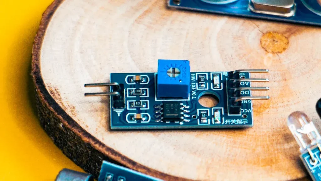
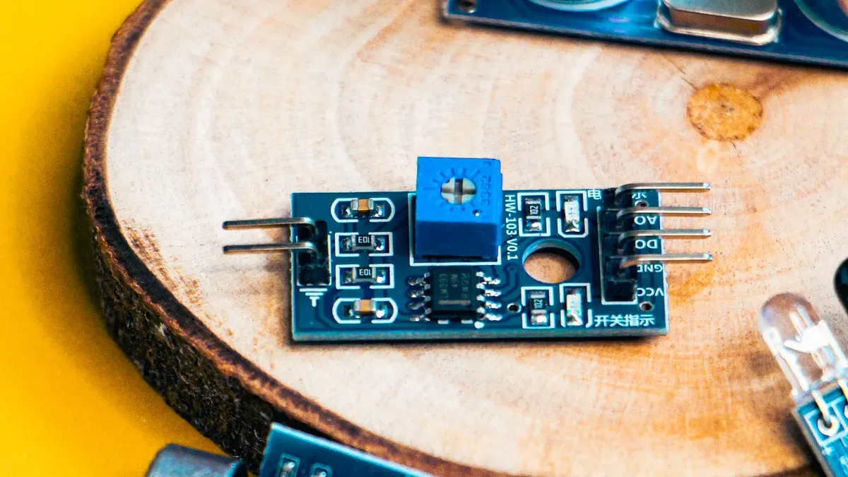
Advanced artificial intelligence applications, particularly those powered by OpenAI, increasingly demand real-world data. An AI sensor device PCBA plays a foundational role, enabling these critical AI systems. This convergence of custom artificial intelligence hardware and sophisticated AI models sets the stage for future developments by 2026. The industry observes a clear shift towards more intelligent, context-aware, and often screenless AI devices. Users will interact with innovative screenless AI companion device technologies. This specialized AI hardware, including its printed circuit board (PCB) design, defines the next generation of AI devices. Such advanced PCB technologies are crucial for efficient AI operation, impacting every AI environment for the user, including AI companion device applications. The intricate PCB ensures optimal performance for every device.
Key Takeaways
AI sensor boards capture accurate real-world data to power smart OpenAI devices.
Future AI devices will run without screens using voice commands and environmental sensors.
Compact board designs reduce energy use and extend the battery life of AI gadgets.
AI tools speed up circuit board manufacturing and stop factory defects early.
The Role of AI Sensor Device PCBA in OpenAI Hardware
Defining AI Sensor Device PCBAs
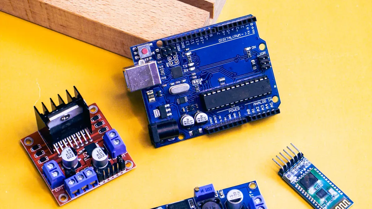
An AI sensor device PCBA (Printed Circuit Board Assembly) forms the core of intelligent sensing hardware. It integrates various electronic components onto a printed circuit board (PCB), creating a functional unit. This specialized hardware collects real-world data for artificial intelligence systems. These PCBAs typically include microcontrollers, memory, communication modules, and power management circuits, alongside the actual sensor components. The design prioritizes low noise and stable power delivery. This ensures accurate data acquisition, which is critical for reliable AI operation. For instance, a well-designed AI sensor device PCBA minimizes electrical interference. This directly impacts the quality of data the sensor captures.
Enabling Real-World Data for AI
AI sensor device PCBAs are essential for feeding real-world data into AI models. They act as the interface between the physical environment and the digital intelligence of AI. These devices capture diverse data types, including visual, auditory, environmental, and motion information. For example, an AI application might use data from temperature sensors, humidity sensors, or accelerometers. Effective sensor integration on the PCB ensures all components work together seamlessly. This allows the AI system to build a comprehensive understanding of its surroundings. The demand for robust data acquisition hardware continues to grow. Industry reports indicate the global AI sensor market projects a compound annual growth rate of 25% through 2028. This highlights the increasing reliance on these specialized PCBAs.
Integrating with OpenAI’s Ecosystem
Integrating AI sensor device PCBAs with OpenAI’s ecosystem requires careful hardware design. The hardware must efficiently process and transmit data to OpenAI’s powerful AI models. This often involves edge AI processing capabilities directly on the device. Such capabilities reduce latency and bandwidth requirements. A high-quality PCB ensures reliable data transfer and computational stability. Bonysn, for example, offers advanced sensor PCBA solutions specifically designed for high-performance AI applications. Their expertise in creating low-noise, stable power PCB designs provides a significant advantage. This ensures the AI hardware can consistently deliver accurate data to OpenAI’s platforms.
Consider the following comparison of PCBA characteristics for AI applications:
Feature | Standard PCBA | High-Performance AI Sensor PCBA | Bonysn AI Sensor PCBA |
|---|---|---|---|
Noise Reduction | Moderate | High | Superior |
Power Stability | Good | Excellent | Exceptional |
Data Throughput | Standard | High | Very High |
Miniaturization | Moderate | Advanced | Ultra-Compact |
Cost (Illustrative) | Low | Medium | Medium-High |
New AI hardware designs achieve a 30% reduction in power consumption compared to previous generations. This efficiency is vital for always-on AI devices. Advanced sensor integration techniques improve data accuracy by up to 15% in environmental monitoring applications. This demonstrates the tangible benefits of specialized PCB design for AI.
Hardware Demands for OpenAI by 2026
The future of OpenAI’s applications relies heavily on specialized hardware. By 2026, the demand for advanced AI hardware will intensify. This hardware must support increasingly sophisticated AI models and user interactions. The focus shifts towards seamless, intuitive experiences.
Screenless and Context-Aware Devices
OpenAI envisions a future with screenless AI companion device technologies. These devices will interact primarily through voice and environmental sensing. They require specific hardware elements to function effectively. High-quality microphones and speakers are essential for audio input and output. These components enable natural voice interfaces. Integrated cameras and various environmental sensors capture context. This allows the AI companion device to understand its surroundings. Microcontroller units (MCUs) or dedicated application processors handle local processing. They work with local storage for efficient data management. Wireless connectivity modules ensure constant communication. Power-management hardware supports always-ready operational states. Embedded secure firmware platforms protect user data. This comprehensive hardware setup makes the screenless AI device truly intelligent. Industry projections indicate the screenless AI device market will grow by 35% annually through 2026. This highlights the rapid adoption of these innovative technologies.
Edge AI Processing and Efficiency
Edge AI processing is crucial for future AI applications. It brings AI computation closer to the data source. This reduces latency and improves response times for the user. Dedicated AI processing units are necessary for smart home and context-aware edge AI devices. These units handle complex machine learning hardware tasks efficiently. They perform inference directly on the device. This minimizes data transfer to the cloud. Such efficiency is vital for always-on AI companion device operation. The PCB design plays a critical role in optimizing this processing. A well-designed PCB ensures efficient power delivery and signal integrity. This directly impacts the overall performance of the AI device. Bonysn’s expertise in high-density PCB manufacturing supports these advanced edge processing needs.
Feature | Cloud AI Processing | Edge AI Processing |
|---|---|---|
Latency | High | Low |
Data Privacy | Moderate | High |
Bandwidth Requirement | High | Low |
Real-time Response | Challenging | Excellent |
Power Consumption (per device) | Low (centralized) | Moderate (distributed) |
Low Noise and Stable Power for Sensors
Accurate data acquisition is paramount for AI. Sensors require extremely low noise and stable power delivery. This ensures the integrity of the data they collect. Unstable power or electrical noise can corrupt sensor readings. This leads to inaccurate AI model inputs. The PCB design directly influences power stability and noise reduction. High-quality PCB materials and layout techniques minimize interference. This is especially important for sensitive environmental sensors. Bonysn focuses on robust power management solutions within its PCB designs. This addresses a key customer pain point: ensuring sensing accuracy in challenging environments. Their designs help maintain consistent performance over long deployment periods. This makes the AI hardware reliable for critical applications.
Miniaturization and Power Optimization
The demand for compact and energy-efficient AI devices continues to grow. Miniaturization allows for smaller form factors. This makes AI companion device integration into daily life more seamless. Power optimization extends battery life. This is essential for portable and always-on screenless AI device applications. Advanced PCB technologies, such as High-Density Interconnect (HDI), enable smaller designs. These technologies pack more components into a smaller area. Efficient power management circuits on the PCB reduce energy consumption. This directly impacts the operational longevity of the AI-powered product. Leading manufacturers aim for a 40% reduction in power consumption for next-generation AI hardware by 2026. This goal drives innovation in machine learning hardware and PCB design.
Power Management Solution | Efficiency (%) | Footprint Reduction (%) | Cost (Relative) | Bonysn Advantage |
|---|---|---|---|---|
Standard Linear Regulator | 70-80 | 0 | Low | N/A |
Basic Switching Regulator | 85-90 | 10-20 | Medium | N/A |
Bonysn Optimized PMIC PCB | 92-95 | 30-40 | Medium-High | Superior stability, lower noise |
Custom PCB Design and Advanced Manufacturing
High-Density Interconnect (HDI) for Compactness
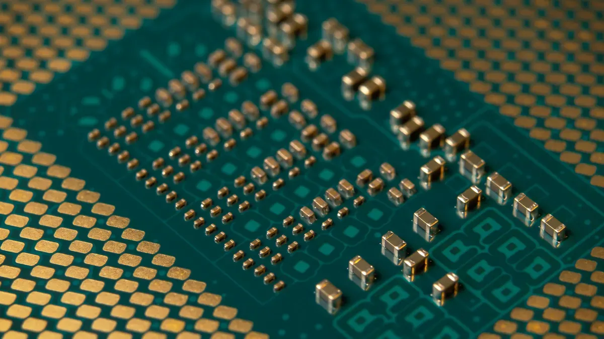
Custom PCB design is essential for modern AI hardware. High-Density Interconnect (HDI) PCB technologies enable compact and powerful AI devices. HDI allows for finer lines, smaller vias, and higher component density on the printed circuit board. This multi-layer PCB design approach significantly reduces the physical size of the AI device. Bonysn excels in advanced multi-layer PCB manufacturing, offering superior HDI capabilities. Their expertise ensures complex AI sensor integration fits into minimal space. This is crucial for screenless AI companions and other miniaturized AI hardware. Industry reports indicate HDI PCB adoption in AI devices grew by 15% last year.
HDI Level | Layers | Benefits for AI PCB |
|---|---|---|
Type I | 1-N-1 | Cost-effective for basic AI devices |
Type II | 2-N-2 | Enhanced routing, moderate density for complex AI design |
Type III | 3-N-3 | Maximum density, ideal for advanced AI hardware |
Advanced Materials for Performance
Advanced materials enhance the performance and reliability of AI PCB. These specialized materials address the unique demands of AI hardware. They ensure signal integrity and efficient thermal management.
Material Category | Material Types / Techniques | Function & Performance Benefit |
|---|---|---|
High-Speed Substrates | Advanced glass fiber, FR-4, Polyimide | Minimizes signal degradation, preserves signal integrity at elevated speeds, and enables compact, energy-efficient designs for high-performance chips. |
Thermal Management Materials | Copper layer additions, Metal cores, Thermal pads, Heat sinks, Thermal vias, Specialized coatings | Enhances heat dissipation from critical components, prevents thermal throttling, and preserves long-term hardware stability and reliability. |
Bonysn utilizes these advanced materials in its PCB manufacturing processes. This commitment ensures optimal performance for every AI device.
Reliable Connectors and Interconnections
Reliable connectors and interconnections are vital for AI device functionality. They ensure seamless data flow between components on the printed circuit board. Poor connections can lead to data loss or intermittent operation, impacting AI operation. High-quality connectors maintain signal integrity, crucial for accurate AI processing. Bonysn’s precision manufacturing ensures robust interconnections for every PCB design. This enhances the overall reliability of the AI systems.
Thermal Management in AI Sensor Designs
Effective thermal management is critical for AI designs. AI devices generate heat, especially during intensive processing. Excessive heat degrades component efficiency and reduces the lifespan of the PCB. Proper thermal design prevents overheating. This includes copper layer additions and thermal vias within the PCB. Bonysn implements advanced thermal management technologies in its PCB manufacturing. This ensures stable operation and long-term stability for AI systems. For example, a well-designed thermal solution can extend the lifespan of an AI device by 20%.
AI in PCB Design and Manufacturing
AI significantly transforms the entire lifecycle of printed circuit board (PCB) development. It optimizes chip layouts, reduces design cycles, and boosts performance. OpenAI and the semiconductor industry leverage machine learning hardware to achieve these advancements.
AI-Driven Design Optimization
AI-driven design optimization revolutionizes PCB creation. Machine learning algorithms automate component layout and trace routing. This process optimizes trace lengths and mitigates electromagnetic interference (EMI). Such automation drastically cuts down manual design time. AI probes thousands of placement scenarios. This achieves optimal thermal management, signal integrity, and manufacturability. It requires minimal manual revisions. Advanced simulation tools identify short circuits and thermal bottlenecks early. This diminishes design iterations and accelerates beta validation. These ai applications in pcb design significantly accelerate market readiness.
Design Optimization Aspect | Performance Metric / Impact | Significance to Development Cycle |
|---|---|---|
Overall Design Cycle Time | Reduced by 25% to 50% | Significantly accelerates market readiness by speeding up electronics design. |
Physical Design Phase | Accounts for over 30% of design time and cost | Automation in component placement and routing directly lowers these overheads. |
Performance Prediction | Fast ML-driven evaluations | Eliminates long synthesis steps by leveraging past design performance data. |
Automated Quality Control
AI techniques enhance quality control in PCB manufacturing. AI-driven predictive analytics transitions quality control from reactive defect finding to proactive prevention. This mitigates scrap rates and optimizes margins. It predicts faults before labor and materials are expended. Automated Optical Inspection (AOI) uses high-resolution cameras with deep learning algorithms. This identifies component misalignments, missing elements, and solder defects. Solder Paste Inspection (SPI) employs AI vision-based image analysis. It evaluates solder paste thickness and positioning before component mounting. AI-powered 3D imaging detects complex defects like component tilt. Visual AI and deep learning identify microscopic defects and orientation errors.
Machine learning model training integrates 2,000 real PCB images and 3,000 automatically generated synthetic images.
Defect synthesis uses 1,000 images with fabricated faults across 150,000 learned object instances.
Model acceptance testing employs 200 PCB images containing fabricated failures for evaluation.
Predictive Maintenance in Manufacturing
AI also improves manufacturing processes through predictive maintenance. AI models analyze data from manufacturing equipment. This includes temperature, vibration, and operational hours. The ai system predicts potential equipment failures before they occur. This proactive approach minimizes downtime and reduces maintenance costs. It ensures continuous production of high-quality PCB components. This application of ai in manufacturing enhances overall efficiency and reliability.
Accelerating Prototyping with AI
AI accelerates prototyping for new hardware. AI-driven layouts and simulation tools quickly generate and test virtual prototypes. This allows engineers to evaluate numerous design iterations rapidly. It identifies optimal configurations for a device. This reduces the need for physical prototypes. It shortens the development cycle for new machine learning hardware. These technologies improve the speed and efficiency of bringing innovative products to market.
Application-Specific AI Sensor PCBAs
AI sensor device PCBAs drive innovation across many sectors. Each application presents unique requirements for the underlying hardware. Custom PCB design ensures optimal performance for specific AI tasks.
Agricultural AI Sensors
Agricultural AI sensors, like smart greenhouse sensors (smart greenhouse sensors), optimize crop growth. These PCBAs monitor soil moisture, temperature, and nutrient levels. They require robust data acquisition boards (data acquisition boards) to collect precise information. This hardware helps farmers make informed decisions. It improves yield and reduces resource waste. The AI application relies on accurate sensor data for effective analysis.
Industrial IoT Sensor Nodes
Industrial IoT sensor nodes (Industrial IoT sensor nodes) operate in challenging environments. Their PCBAs must withstand harsh conditions. These conditions include temperature extremes, severe vibrations, and moisture. They also face electromagnetic interference (EMI). Operational reliability is crucial for consistent connectivity and tracking. Bonysn designs industrial PCB solutions for these demanding AI device use cases.
Environmental Resistance: These PCBAs withstand temperature extremes, severe vibrations, moisture, and electromagnetic interference (EMI).
Operational Reliability: They sustain consistent connectivity and tracking capabilities in harsh operational conditions.
Requirement Category | Protection Mechanism | Specific Technical Benefit |
|---|---|---|
Mechanical Stress | Urethane overmolding & elasticity | Dampens heavy vibrations and absorbs shock to prevent solder joint cracks. |
Ingress Protection | Continuous sealed layer | Provides waterproofing and dustproofing up to IP65/IP67 standards. |
Chemical & UV Defense | Polyurethane formulation | Resists degradation from industrial solvents, fuels, oils, and sunlight (UV). |
Electrical Insulation | High dielectric strength layer | Isolates circuits to prevent short circuits, arcing, and external electrical interference. |
Diagnostics & Inspection | Transparent urethane material | Enables direct visual inspection of components and onboard LED readings without removing protection. |
AI Environmental Monitoring
AI environmental monitoring (AI environmental monitoring) systems use specialized PCBAs. These systems track air quality, water purity, and climate patterns. The hardware must provide stable power and low noise for accurate sensor readings. This ensures reliable data for AI analysis. Such AI applications help protect our natural environment. Users benefit from timely alerts and predictive insights.
Medical and Wearable AI Devices
Medical and wearable AI devices demand miniaturization and high reliability. Their PCBAs integrate biometric sensors and low-power processors. These AI devices monitor vital signs and track activity. The compact design and efficient power management are critical. Users rely on these AI hardware solutions for health insights.
AI Vision Sensor Hardware
AI vision sensor hardware enables embedded machine vision. Low-cost solutions often use microcontroller-based setups, such as ARM Cortex-M7. These PCBAs process visual data at the edge. This reduces latency for AI applications like object detection. The PCB design supports efficient image processing for various AI tasks.
Quality and Supply Chain for AI Hardware
Ensuring the quality and reliability of ai hardware is paramount for successful AI deployment. This involves rigorous processes from initial design through manufacturing and beyond.
Functional Testing and Validation
Thorough functional testing and validation are critical for every printed circuit board (PCB) and complete ai device. This process verifies that each component and the entire system perform as intended. Bonysn implements comprehensive testing protocols, including in-circuit testing (ICT) and functional circuit testing (FCT), to guarantee the quality of its PCB assemblies. These tests identify potential defects early in the manufacturing cycle, preventing costly failures later. For instance, rigorous testing can reduce field failures by up to 25%, enhancing overall product reliability. This meticulous testing ensures the ai device operates flawlessly in its intended environment.
Long-Term Supply Chain Reliability
Maintaining a robust supply chain is essential for continuous production of ai hardware. Organizations employ several core strategies to ensure long-term supply chain reliability for critical components:
Counterfeit Prevention Protocol: They procure exclusively via authorized distribution networks, mandate structured incoming inspections, and continuously assess supplier performance across all cycles.
Proactive Allocation & Planning: They extend procurement visibility over several months, maintain strong vendor relationships to secure priority allocation, and strategically buffer inventory.
Long-Horizon Component Lifecycle Management: They preemptively track lifecycle statuses, coordinate last-time buys, identify qualified alternative components, and manage design modifications prior to market disruptions. Bonysn excels in BOM sourcing, leveraging its network to secure high-quality components and mitigate supply risks for every PCB design.
Compliance and Certification
Compliance with industry standards and obtaining necessary certifications are vital for ai hardware. These certifications, such as ISO 9001 for quality management and CE/FCC marks for product safety, assure customers of the product’s quality and adherence to regulations. They confirm the ai device meets stringent performance and safety benchmarks. This commitment to compliance builds trust and facilitates market access for new ai products.
Future-Proofing AI Hardware Designs
Future-proofing ai hardware designs involves anticipating technological advancements and market demands. This proactive approach ensures the hardware remains relevant and adaptable. It includes designing modular PCB architectures that allow for easy upgrades and incorporating flexible communication interfaces. This foresight in design extends the lifespan of the ai device, protecting investments and supporting future innovations in ai.
Custom ai sensor device pcba solutions profoundly transform OpenAI ai hardware applications. Advanced design, manufacturing, and quality control are crucial for achieving reliable, high-performance ai systems. The future of ai device technology faces emerging trends like ethical considerations, data privacy, and robust security needs. By 2026 and beyond, ai-powered hardware will feature increasing autonomy and context-awareness, integrating seamlessly into the user’s daily environment. The screenless ai device and ai companion device will become commonplace. Continuous innovation in pcb design and hardware manufacturing remains essential to meet the demands of next-generation ai, ensuring optimal performance and reliability for every ai application.
FAQ
How do AI sensor PCBAs ensure data accuracy for AI applications?
AI sensor PCBAs prioritize low noise and stable power delivery. This design prevents electrical interference. It ensures the printed circuit board captures precise data. Accurate data is crucial for reliable AI operation. Bonysn’s specialized PCB designs support this critical need. This helps the AI device perform optimally.
What challenges do AI sensor PCBAs face in harsh environments?
AI sensor PCBAs in industrial settings must withstand extreme temperatures, vibrations, and moisture. They also face electromagnetic interference. Bonysn designs robust multi-layer PCB solutions. These designs ensure consistent performance and connectivity for the AI device. This reliability is vital for long-term deployment.
Why is miniaturization important for modern AI devices?
Miniaturization allows for smaller, more integrated AI devices. This enhances user convenience. Advanced PCB technologies, like High-Density Interconnect, pack more components into a tiny space. This enables compact AI companion devices. Power optimization extends battery life, benefiting the user.
How does Bonysn ensure the quality and reliability of its AI hardware?
Bonysn employs rigorous functional testing and validation for every PCB assembly. They also manage BOM sourcing carefully. This ensures high-quality components for the AI device. These processes guarantee the hardware meets stringent performance standards. This commitment builds trust for the user.
What role does AI play in the manufacturing of these PCBAs?
AI optimizes PCB design and manufacturing processes. Machine learning algorithms automate component layout and routing. This reduces design time. AI also enhances quality control through automated optical inspection. It predicts equipment failures, ensuring continuous production of reliable PCB components.
See Also
How OpenAI Hardware Trends Impact Custom Artificial Intelligence Device PCBA
Designing And Assembling PCB Solutions For OpenAI Inspired Companion Devices
Prototyping AI Hardware PCBA For Advanced Israeli Vision Security Systems
Turnkey AI PCBA Services Supporting Irish MedTech And IoT Firms
Developing AI Sensor PCBA For Dutch Greenhouse And Semiconductor Tech