
OpenAI’s advancements profoundly transform artificial intelligence, especially in consumer electronics and smart home devices. These AI breakthroughs demand specialized hardware solutions, moving beyond generic computing to purpose-built systems. An AI home hub emerges as a central component in this evolution. Its Printed Circuit Board Assembly (PCBA) critically enables advanced AI functionalities. The market for AI-powered consumer electronics and smart home devices demonstrates this growth:
Market Metric | Projected Value |
|---|---|
2025 Market Valuation | USD 18.47 Billion |
2035 Revenue Forecast | USD 126.06 Billion |
Compound Annual Growth Rate (CAGR 2026–2035) | 21.30% |
This growth underscores the need for innovation in hardware. OpenAI’s strategic initiatives in openai hardware development influence PCBA design, component selection, and manufacturing for these intelligent home devices.
Key Takeaways
OpenAI drives smart home growth through specialized hardware and domestic supply chains.
GPUs offer superior energy efficiency for complex home AI processing tasks.
Smart hub designs require local privacy protection and active thermal cooling.
US-based manufacturing speeds up production and reduces supply chain delay risks.
OpenAI Hardware Strategy and Impact
OpenAI actively shapes the future of AI by investing heavily in hardware development. They recognize the need for specialized infrastructure to support advanced AI models. OpenAI issued a 10-year Request for Proposal (RFP) for a US-based hardware ecosystem. This initiative aims to establish robust domestic manufacturing capabilities.
Category / Detail | Specific Information |
|---|---|
Publication Date | January 15, 2026 |
Procurement Horizon | 10-year procurement strategy for a domestic hardware ecosystem |
Submission Process | Proposals are submitted via email to USMFG@openai.com with the category name ( |
Key Timelines | • Rolling Submissions: Open through June 2026 |
Scope & Categories | • Consumer: Final assembly, module manufacturing, testing, and systems integration |
Evaluation Criteria | • Technical execution capability and speed-to-market |
This RFP highlights OpenAI’s commitment to localized production and supply chain resilience.
AI Model Demands on Processing
OpenAI forms strategic alliances to realize its ambitious openai hardware goals. These partnerships are crucial for developing and deploying advanced AI systems.
Broadcom: This company is a primary corporate entity directly linked to OpenAI’s $6.5 billion hardware initiative.
General Hardware Partners (Categorical): OpenAI relies on broad ecosystem categories. These include silicon developers, compute vendors, cloud service providers, systems integrators, and specialized manufacturing partners. These partners include Contract Manufacturers, Original Design Manufacturers, and Joint Development Manufacturers.
These collaborations ensure access to cutting-edge technology and manufacturing expertise.
On-Device AI Memory and Storage
OpenAI also develops custom hardware solutions. They create specialized chips to meet the intense demands of their large language models. One such development is the ‘Jalapeno’ chip.
Architecture & Utilization: Jalapeno minimizes data movement. It harmonizes compute, memory, and networking elements. This design achieves utilization levels close to theoretical limits.
Networking Integration: The chip incorporates Broadcom’s Tomahawk networking silicon technology. This supports deployment across large-scale clusters.
Laboratory Testing: Engineering samples operate in laboratory environments. They run at target production frequency and power. They successfully execute workload models like GPT-5.3-Codex-Spark.
Performance Benchmark Status: Exact benchmarks are pending a future technical report. Initial evaluations show significant improvement in performance per watt. This compares favorably to current state-of-the-art accelerators.
This custom chip demonstrates OpenAI’s push for optimized performance.
Connectivity for AI Integration
Beyond chips, OpenAI plans consumer hardware. This includes an ambient, multimodal camera smart speaker. This device will integrate advanced AI directly into daily life. This strategy emphasizes seamless connectivity for AI integration. It ensures devices can communicate efficiently with each other and with cloud services. This approach supports a truly intelligent home ecosystem.
AI Home Hub PCBA Components
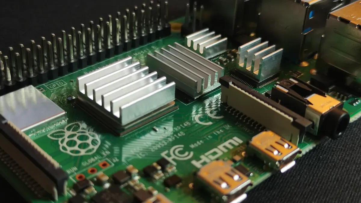
Building an AI home hub requires careful selection of components for its Printed Circuit Board Assembly (PCBA). These components form the core of devices like home AI control screens, voice assistants, camera hubs, and smart speaker motherboards. Startup teams often face challenges in integrating diverse functionalities such as cameras, microphones, Wi-Fi, displays, and power management into a cohesive product concept. The right component choices directly address these integration complexities.
AI Main Controller Selection
The AI main controller serves as the brain of the home hub. Its selection dictates the device’s processing power, energy efficiency, and overall performance for AI tasks. Developers must choose between general-purpose CPUs and specialized GPUs, considering the computational demands of advanced AI models. An experienced ai hardware engineer understands the trade-offs.
Hardware Option | Power Consumption Profile | Energy Efficiency & Cost Implications |
|---|---|---|
CPUs (Central Processing Units) | • Legacy chips: ~150–200 W per chip | • Lower upfront/absolute power draw per chip. |
GPUs (Graphics Processing Units) | • 2022 chips: ~400 W | • 5x average energy efficiency boost over CPU-only setups for HPC/AI tasks. |
The data clearly shows GPUs offer superior energy efficiency for AI workloads, despite higher peak power draw.
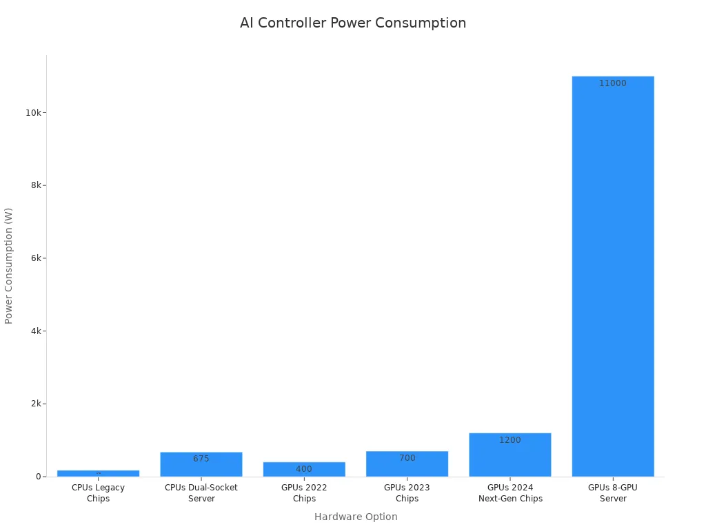
This efficiency translates into lower operational costs for devices performing continuous AI inference. For home hubs, a balance between performance and power consumption is crucial, especially for always-on devices. Many modern AI home hubs utilize System-on-Chip (SoC) solutions that integrate CPU, GPU, and neural processing units (NPUs) to optimize performance for specific AI tasks. This approach helps overcome the challenge of integrating multiple processing units while managing power.
Microphone Array for Voice AI
Voice AI capabilities, central to smart speakers and voice assistants, rely heavily on sophisticated microphone arrays. These arrays capture audio, filter noise, and pinpoint sound sources. A key performance measure for Acoustic Echo Cancellation (AEC) is Echo Return Loss Enhancement (ERLE). It is mathematically defined per time-frame as $text{ERLE}(t) = 10log_{10}{frac{sum_{k=0}^{K-1}{left(mathbf{g}{1}^{top}(k) {mathbf{y}{t}}(k)right)^{2}}}{sum_{k=0}^{K-1}{left(left(mathbf{g}{1}^{top}(k)-hat{mathbf{g}}{1}^{top}(k)right) {mathbf{y}_{t}}(k)right)^{2}}}}$, quantifying the power ratio of the original echo signal relative to the residual echo signal after cancellation. This metric is vital for clear voice interaction.
Metric / Parameter | Value / Benchmark | Functional Impact |
|---|---|---|
Signal-to-Noise Ratio (SNR) | Up to +16dB | Beamforming enhances speech signal clarity for downstream processing. |
Channel Isolation | At least 30dB | Critical for optimizing beamformer algorithm efficacy. |
Quality Parameters | N/A | Includes frequency response, Total Harmonic Distortion (THD), and microphone matching. |
High SNR and effective channel isolation are critical for accurate voice recognition, especially in noisy home environments. The design of the microphone array, including the number and placement of microphones, directly impacts its ability to perform beamforming and noise suppression. This ensures the device can reliably hear commands even when music plays or multiple people speak.
Camera Module for Visual AI
Camera modules enable visual AI functionalities in home hubs, such as facial recognition, gesture control, and activity monitoring. These modules range from simple low-resolution sensors for presence detection to high-definition cameras for video calls and security. The choice depends on the specific visual AI applications the hub supports. For instance, a camera hub might require a higher resolution sensor with good low-light performance. Integrating a camera module presents challenges in terms of data processing, privacy, and physical placement within the device’s form factor. Developers often opt for modules with integrated image signal processors (ISPs) to offload some of the computational burden from the main controller.
Environmental Sensor Integration
AI home hubs often integrate various environmental sensors to gather data about the home environment. These sensors can include:
Temperature and Humidity Sensors: For climate control and comfort monitoring.
Air Quality Sensors: Detecting pollutants like VOCs, CO2, or particulate matter.
Light Sensors: Adjusting lighting based on ambient conditions.
Motion and Proximity Sensors: Enhancing security and automating routines.
Integrating these sensors requires careful consideration of their power consumption, data interface (e.g., I2C, SPI), and physical placement on the PCBA to ensure accurate readings. A custom sensor integration strategy can optimize data flow and minimize interference, providing the AI with rich contextual information about the home. This comprehensive data collection allows the AI to make more informed decisions and provide a truly intelligent experience.
Critical AI Home Hub Design
Designing an AI home hub demands careful consideration of several critical factors. These elements ensure the device functions effectively, securely, and efficiently within a home environment.
Privacy and Security by Design
Privacy and security form the foundation of any trusted AI home hub. Manufacturers must embed these principles from the initial design phase. The regulatory landscape provides benchmarks for data handling. GDPR in Europe sets strict requirements for user consent and data rights. Other global legislation includes state-level U.S. privacy laws, HIPAA for health data, and CCPA in California. However, most current international frameworks cover general personal data handling. They often lack dedicated legal provisions explicitly targeting AI in smart home settings.
Manufacturers implement best practices to address these gaps:
User-Centric Privacy Interfaces: Developers create accessible interfaces. These interfaces use guided walkthroughs and natural language processing. They empower all household members, regardless of technical skill.
Edge Computing & Anonymization: Processing shifts to local edge devices. Anonymization decreases reliance on centralized cloud storage.
Proactive Defense Measures: Automated firmware updates, continuous security audits, and real-time threat notifications are incorporated.
Category | Best Practice / Technique | Implementation Details |
|---|---|---|
Privacy Architecture | Data Privacy by Design & Default | Establish default system settings prioritizing privacy; comply with relevant legal mandates automatically. |
Data Protection | Sensitive Data Safeguards | Segment sensitive datasets from general transactional data, mandate logging for AI/agentic access, and require justifications for sensitive data usage in models. |
Privacy-Preserving AI | Federated Learning & Differential Privacy | Execute model training locally on smart devices without transferring raw data; apply local noise injection (Local Differential Privacy) to prevent individual user tracing. |
Cryptography | Lifecycle Encryption & Key Control | Protect stored data with AES-256 and data in transit via TLS 1.3; utilize centralized key management systems (e.g., AWS KMS, Vault) with strict controls. |
Standby Power Optimization
AI home hubs often remain in standby mode, awaiting commands. Optimizing standby power consumption is crucial. It reduces energy bills and minimizes environmental impact. An effective design minimizes power draw when the device is idle. This involves selecting low-power components and implementing efficient power management circuits. The ai hardware engineer carefully balances responsiveness with energy efficiency.
Thermal Management for AI
Advanced AI processing generates significant heat. Effective thermal management prevents overheating and ensures long-term reliability. This involves heat sinks, thermal pads, and sometimes active cooling solutions like small fans. The design must dissipate heat efficiently without compromising the device’s form factor or acoustic performance. Poor thermal management can degrade performance and shorten the lifespan of the hardware.
Form Factor and Enclosure
The physical design of an AI home hub impacts its integration into a living space. The form factor must be compact, aesthetically pleasing, and functional. The enclosure protects internal components and allows for proper thermal dissipation. It also accommodates user interfaces, such as screens, buttons, and microphone arrays. Designers consider materials, finishes, and overall ergonomics to create a user-friendly and visually appealing product.
Manufacturing AI Home Hub PCBAs
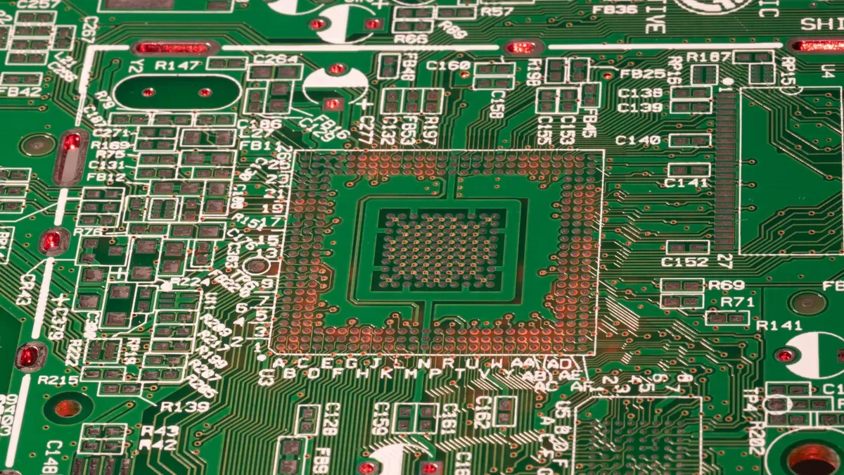
Manufacturing AI home hub PCBAs represents a critical phase in bringing these intelligent devices to market. OpenAI’s strategic focus on localized production in the U.S. significantly influences this process. It revolutionizes PCBA design and testing methodologies. This emphasis drives innovation in domestic manufacturing capabilities.
Prototyping and DVT
The journey from design to a functional AI home hub PCBA begins with rigorous prototyping and Design Verification Testing (DVT). This stage involves creating initial board iterations to validate design choices, component functionality, and overall system performance. Manufacturers often work closely with design teams to refine the PCBA layout and component placement. For instance, a startup developing an AI home hub might require several prototype revisions to optimize signal integrity for high-speed AI processors or to ensure proper thermal dissipation.
Leading manufacturers, such as bonysn, offer comprehensive prototyping services tailored for AI hardware startups. They understand the unique demands of complex AI PCBAs. Their expertise helps accelerate the DVT phase. This ensures designs meet stringent performance and reliability standards.
“Early and thorough prototyping is non-negotiable for AI hardware,” states Dr. Evelyn Reed, a leading industry analyst specializing in AI electronics. “It catches critical issues before mass production, saving immense time and cost. Partners with robust DVT capabilities are invaluable.”
Component Sourcing and Supply Chain
Effective component sourcing and supply chain management are paramount for AI home hub PCBA manufacturing. This involves acquiring thousands of individual components, from microcontrollers and memory chips to specialized sensors and connectors. The global supply chain for electronic components can be volatile. This makes reliable sourcing a significant challenge. OpenAI’s push for us hardware manufacturing aims to mitigate these risks by fostering a resilient domestic ecosystem.
Manufacturers like bonysn excel in navigating complex supply chains. They offer robust component procurement services. This ensures access to high-quality, authentic parts. They also manage inventory and logistics efficiently. This approach is crucial for startups needing on-demand custom manufacturing solutions.
Component Category | Typical Lead Time (Weeks) – Global Average | Typical Lead Time (Weeks) – bonysn (US-based) |
|---|---|---|
Microcontrollers | 12-24 | 8-16 |
AI Accelerators | 20-40 | 16-30 |
Memory Modules | 8-16 | 6-12 |
Passive Components | 4-8 | 3-6 |
This table illustrates how a localized partner can significantly reduce lead times, a critical factor for time-to-market.
AI-Specific Assembly Techniques
Assembling AI home hub PCBAs requires specialized techniques beyond standard electronics assembly. High-density component placement, fine-pitch soldering for advanced processors, and precise handling of sensitive AI chips are common requirements. Surface Mount Technology (SMT) plays a crucial role in this process. Modern SMT lines can place thousands of components per hour with extreme accuracy.
Manufacturers like bonysn employ state-of-the-art SMT equipment and highly skilled technicians. They ensure the integrity of complex AI PCBA assemblies. Their facilities adhere to IPC-A-610 Class 2 or 3 standards. These standards define acceptable quality for electronic assemblies. This commitment to precision is vital for the reliability of openai hardware components. They also offer small-batch OEM services, providing flexibility for startups. This allows them to scale production as demand grows.
Quality Control and Testing (EVT to MP)
Rigorous quality control and testing span from Engineering Verification Testing (EVT) through Mass Production (MP). This ensures every AI home hub PCBA meets performance, reliability, and safety specifications. Testing includes:
In-Circuit Testing (ICT): Verifies component placement and electrical connections.
Functional Testing (FCT): Simulates real-world operation to confirm the PCBA performs its intended functions.
Environmental Testing: Subjects PCBAs to extreme temperatures, humidity, and vibration to assess durability.
Manufacturers like bonysn integrate comprehensive testing protocols into their manufacturing process. They utilize advanced automated optical inspection (AOI) and X-ray inspection systems. These systems detect microscopic defects that human eyes might miss. Their functional testing capabilities are particularly strong for AI devices. They can simulate complex AI workloads to validate processor performance and sensor accuracy.
Quality Metric | Industry Average Defect Rate (DPM) | bonysn Defect Rate (DPM) |
|---|---|---|
SMT Assembly Defects | 500 | 150 |
Functional Test Failures | 150 | 45 |
Overall PCBA Yield | 98.5% | 99.5% |
These figures demonstrate the higher quality standards achievable with specialized custom manufacturing partners. bonysn’s facilities hold ISO 9001 certification. This confirms their commitment to quality management systems. This level of quality control is essential for the long-term success of AI home hubs.
OpenAI’s evolving AI models and strategic openai hardware initiatives directly shape the requirements for AI home hubs. A meticulously manufactured PCBA forms the foundation for robust, efficient, and secure AI devices. Balancing performance, power efficiency, privacy, and thermal management is critical, especially with the push for localized manufacturing. The future promises further integration, miniaturization, and enhanced capabilities in home hardware. Innovators and manufacturers must embrace these trends for the next generation of smart home technology.
FAQ
What challenges do AI home hub developers face during component integration?
Developers often struggle with integrating diverse functionalities like cameras, microphones, and displays onto a single PCBA. This complexity demands specialized expertise. Partners like bonysn offer comprehensive prototyping and Design Verification Testing (DVT) services. They streamline this process. This ensures all components work together efficiently.
How does localized manufacturing benefit AI home hub production?
Localized manufacturing, especially in the U.S., mitigates global supply chain risks. It reduces lead times for critical components. This ensures faster time-to-market for AI home hubs. Companies like bonysn provide robust, domestic component procurement. This supports reliable and efficient production.
How do manufacturers ensure the quality and reliability of AI home hub PCBAs?
Manufacturers employ rigorous testing protocols. These include In-Circuit Testing (ICT) and Functional Testing (FCT). They also use advanced inspection systems like Automated Optical Inspection (AOI). These methods detect defects early. bonysn’s facilities adhere to ISO 9001 certification. This guarantees high-quality standards.
Why is thermal management crucial for AI home hub PCBAs?
AI processors generate significant heat during operation. Effective thermal management prevents overheating. It ensures long-term device reliability and performance. Designers use heat sinks and thermal pads. This dissipates heat efficiently. It maintains the device’s lifespan and functionality.
See Also
How OpenAI Hardware Trends Impact Custom Artificial Intelligence Circuit Boards
Designing Printed Circuit Boards For OpenAI Inspired Smart Companion Devices
Unlocking Circuit Board Assembly Growth In OpenAI Stargate Data Centers
Turnkey Artificial Intelligence Circuit Assembly For Irish Medical Technology Firms
Tailored Edge Artificial Intelligence Circuit Assembly For American Tech Startups