The AI hardware market is experiencing rapid growth, placing critical importance on robust and high-quality PCBA assembly. AI hardware startups encounter unique challenges. These include rapid innovation cycles, complex designs, and the vital need for reliable domestic supply chains. Specialized PCBA assembly services in the USA offer a significant competitive advantage to these emerging companies. These services are uniquely positioned to support startups. They ensure advanced PCBA manufacturing for products like AI edge boxes and GPU expansion boards. This blog will explore how US-based providers empower AI hardware innovation. It will also discuss future trends and strategic advantages in the sector.
Key Takeaways
Advanced HDI PCB technology enables compact designs for powerful AI devices.
US manufacturers reduce supply chain delays from eight weeks to two weeks.
Domestic production protects valuable intellectual property and lowers product defect rates.
Smart factory automation uses artificial intelligence to inspect circuit boards with extreme precision.
Advanced PCBA for AI Hardware
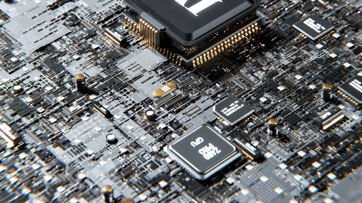
AI hardware demands specialized PCBA assembly to meet its rigorous performance and miniaturization requirements. These technological advancements are crucial for devices such as AI edge boxes, GPU expansion boards, smart cameras, and voice devices. The complexity of AI applications drives innovation in printed circuit board (PCB) design and manufacturing processes. This ensures that the underlying hardware can support high-speed data processing and compact form factors.
High-Density PCB and Miniaturization
Miniaturization is a key factor for AI hardware, especially for edge devices and embedded systems. High-density interconnect (HDI) PCB technology enables this compact design. HDI PCBs feature finer lines, smaller vias, and higher component density. This allows engineers to pack more functionality into a smaller space. For example, 1+N+1 HDI technology uses single-step microvias and offers a lower cost solution for moderate AI edge boards. More complex designs, like 2+N+2 HDI, incorporate two microvia layers, providing better density for GPU and AI module breakout. For extreme density in AI accelerator boards, 3+N+3 HDI offers three microvia layers, though at a higher cost.
Every Layer Interconnection (ELIC) technology allows microvias on every layer, which is critical for ultra-dense AI packages and GPU BGA escape. Ultra HDI pushes boundaries further with sub-30 μm routing, supporting very dense packages and high-speed SerDes breakout. Microvias, with diameters typically between 75–100 μm, are laser-drilled. They facilitate fine-pitch BGA fan-out and High Bandwidth Memory (HBM) connections. Fine trace/space capabilities, reaching 50/50 μm and even 30/30 μm, enable high-density routing under 0.4 mm pitch BGAs. Sequential lamination, involving repeated laser drilling and copper filling, creates stacked microvias for multi-layer HDI. Controlled impedance, such as 50 Ω single-ended and 85/90/100 Ω differential, ensures signal integrity for high-speed interfaces like PCIe Gen5/6 and DDR5/6. Standard trace width and spacing for PCBs are often 4 mil/4 mil without severe cost penalties. However, extreme manufacturing limits can achieve 3 mil/3 mil for complex HDI projects. For ultra-thin, high-density applications, laser drilling microvia technology supports 2 mil/2 mil (0.05 mm). High-layer-count PCBs, sometimes exceeding 24 layers, are common in AI GPUs, servers, and accelerators for robust signal integrity.
Complex Component Integration
AI hardware relies heavily on the precise integration of complex components onto the PCBA. Modern AI modules often feature fine-pitch BGA packages, System-on-Module (SoM) solutions, tiny passive elements, and integrated circuits (ICs) with high pin counts. These components demand advanced PCBA assembly techniques and stringent quality control. The intricate nature of these parts requires specialized equipment and expertise during the assembly process.
High-density routing, fine-pitch BGAs, and embedded processors are increasingly used in high-performance edge computing devices. BGA packages are widely used in AI and data center hardware. This includes GPU accelerators, FPGA boards, and high-performance computing modules. The precise placement and reflow soldering of these components are critical for the functionality and reliability of the final AI product. Proper thermal management and signal integrity considerations are also paramount during the PCBA assembly of these complex parts.
US PCBA Manufacturing Advantages
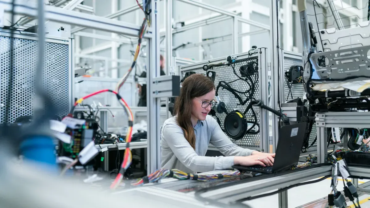
US AI hardware companies often choose domestic PCBA manufacturing for several compelling reasons. These include intellectual property protection and robust supply chain stability. Domestic production offers a competitive edge, ensuring that advanced AI hardware, such as AI edge boxes and GPU expansion boards, meets stringent requirements.
Supply Chain Resilience and Security
A resilient supply chain is critical for AI hardware startups. They face rapid innovation cycles and complex designs. Overseas PCBA factories often present significant challenges. For example, 80% of AI startups report delays of 7 to 9 weeks in motherboard delivery. The average lead time for high-end HDI samples and small-batch production extends to 8 weeks, compared to a standard 2-4 weeks. Small-batch trial production also requires line reconfiguration, increasing costs by up to 60%. Furthermore, 40% of PCBA factories cannot manufacture server boards due to insufficient lamination and microvia capabilities. Geopolitical tensions also increase import lead times and costs by over 30%, with 70% of capacity concentrated in Taiwan and South Korea.
The supply chain crisis continues, with parts becoming available and then disappearing quickly. This creates a cycle where companies try to design around shortages, which is expensive and often ineffective. US-based electronics manufacturing mitigates these risks. A “Design for Volatility” program, for instance, incorporates alternate sourcing strategies, approved vendor list development, and lifecycle planning into every production program. This means a Bill of Materials (BOM) is optimized not just for today’s component availability. It is structured to absorb supply shocks, end-of-life events, and tariff exposure without stopping the production line.
Domestic PCBA manufacturing offers clear advantages in mitigating supply chain risks:
Risk | Mitigation |
|---|---|
Long lead times | Component substitution with domestic alternatives reduces lead time from 8 weeks to 2 weeks, and lowers cost by 20% |
Component shortages | Established supplier relationships enable quick sourcing of necessary parts even during shortages |
Counterfeit parts | Component traceability reports allow verification of batch numbers, ensuring authenticity |
Quality inconsistencies | Comprehensive material traceability and digitized processes (e.g., temperature/humidity monitoring, electronic tags) lock out expired materials |
Production delays | Rapid reconfiguration of production lines handles sudden material shortages or design tweaks on the fly |
Inflexibility | Small-batch manufacturing and cloud-based collaboration platforms support frequent design iterations |
Price volatility | Long-term supplier relationships secure stable chip pricing |
Poor communication | Transparent production model with real-time video feeds and online engineering sample approval |
This level of control and flexibility is vital for AI hardware startups. It ensures a stable and secure supply chain for their pcba assembly needs.
Regulatory Compliance and Quality
US PCBA manufacturing adheres to strict regulatory standards and maintains high quality benchmarks. This is crucial for AI hardware, which often involves sensitive technology. Manufacturers must comply with RoHS (Restriction of Hazardous Substances) and REACH (Registration, Evaluation, Authorization, and Restriction of Chemicals) for hazardous substance restrictions. UL certification ensures product safety. IPC standards govern the quality and reliability of electronic assemblies. Additionally, ITAR (International Traffic in Arms Regulations) and EAR (Export Administration Regulations) are required for defense-related products. Holding ISO 9001:2015 certification further demonstrates a commitment to quality management. Non-compliance with these regulations can lead to fines, product recalls, market bans, or criminal penalties.
ITAR is a U.S. government standard controlling the export and import of defense-related articles, including PCBs for military or AI hardware applications. US PCBA manufacturers must register with the Directorate of Defense Trade Controls (DDTC). They must protect controlled technical data, such as design specifications and manufacturing processes. They also need export licenses before sharing such information with foreign entities. This protects intellectual property and national security.
US electronics manufacturing also boasts superior quality. The National Institute of Standards and Technology (NIST) reports that U.S. electronics manufacturers have defect rates 40–60% lower than comparable offshore facilities. This higher quality translates to faster time-to-market. Collaborative design support, such as Design for Manufacturability (DFM) consultations, optimizes PCB layouts for cost, space, and power. Rapid prototyping capabilities allow for quicker turnaround of working prototypes. This reduces time to market. Advanced capabilities, including rigid-flex PCBs, embedded electronics, and multi-layer boards, are engineered for compact form factors. Unlike many foreign competitors, US pcba factories are not subject to export-control restrictions. This limits access to the most advanced U.S. technologies.
Quality control metrics are essential for AI hardware pcba. First Pass Yield (FPY) measures the percentage of units passing a single process step without rework. Rolled Throughput Yield (RTY) calculates the probability a unit passes every step cleanly. For example, five stations at 95% FPY result in an RTY of only 77.4%. This exposes hidden factory issues.
Here are FPY benchmarks:
Board Type / Condition | FPY Benchmark |
|---|---|
Mature PCB lines | 95–98% |
Best-in-class steady state | 98.5%+ |
Complex multi-layer / HDI | 92–95% |
Below 92% in stable production | Indicator of structural issues |
The Six Sigma target of 99.99966% FPY is equivalent to 3.4 defects per million opportunities (DPMO). This high standard for pcba assembly ensures the reliability of critical AI hardware.
Tailored PCBA Assembly Services for Startups
Specialized PCBA assembly services cater directly to the unique needs of AI hardware startups. These services offer a comprehensive, one-stop solution from initial design files to fully tested products. This approach addresses the market demand for seamless transitions from Gerber files and Bill of Materials (BOM) to prototyping, small-batch production, and functional testing. Startups often face pain points like rapid prototype iteration, complex BGA and high-speed interfaces, and a lack of cooperative manufacturing teams. US-based electronics manufacturing partners provide the necessary support to overcome these challenges.
Rapid Prototyping and DFM
Rapid prototyping is essential for AI hardware startups, allowing them to quickly iterate on designs and validate concepts. US PCBA factories offer accelerated turnaround times for various categories. For instance, IC evaluation boards can go from weeks to hours, and design validation boards from months to days. Backplane and interconnect boards, which once took over 30 days, can now be produced in under 24 hours. Semiconductors and consumer electronics can see first candidates within one hour of a single workday. Robotics prototypes can be delivered in under one day, down from four weeks. PCB designers can achieve a full fab-ready design in under four hours, and electrical engineers can go from schematic to fab-ready in the same timeframe. General prototyping services deliver boards weekly, with schematic-to-board processes completed in hours. This speed is critical for maintaining rapid innovation cycles.
Design for Manufacturability (DFM) is another crucial service. It optimizes PCB layouts for cost, space, and power, ensuring that designs are not only functional but also efficient to produce. This collaborative design support helps startups avoid costly redesigns and delays. For a PCBA assembly quotation, startups typically need to provide specific documents. These include a Bill of Materials (BOM), Gerber files, and a Centroid file (also known as a pick-and-place file or CPL). These documents allow the PCBA factories to accurately assess the project requirements and provide precise quotes.
Flexible Production and Scaling
AI hardware startups require flexible production capabilities that can scale from early prototypes to small-batch trial production and eventually to mass production. US-based PCBA assembly services excel in this area, offering the agility needed for evolving AI hardware designs. They support rapid PCB prototyping, efficient BOM procurement, Surface Mount Technology (SMT) assembly, X-Ray inspection, and comprehensive functional testing. These capabilities directly address the pain points of rapid prototype iteration and the need for cooperative manufacturing teams.
The production process typically involves distinct phases: Engineering Validation Test (EVT), Design Validation Test (DVT), and Production Validation Test (PVT). Each phase has a specific purpose and set of tests. EVT validates the core engineering architecture and components through bench validation, firmware bring-up, power profiling, and early thermal checks. The exit signal for EVT is when main functions meet the Product Requirements Document (PRD). DVT validates the near-final design under real-world conditions, including drop, vibration, thermal cycling, Highly Accelerated Life Test (HALT), and certification testing. DVT concludes when the design passes with limited fixes. PVT validates manufacturing process repeatability and quality through line tests, fixture validation, yield tracking, and packaging checks. The PVT exit signal indicates the factory can build shippable units repeatedly. EVT proves the engineering works, DVT proves the design survives real use, and PVT proves the factory can build it reliably at scale. This structured approach ensures high-quality PCBA production and efficient scaling for AI hardware. The flexibility in production allows startups to adapt quickly to market changes and technological advancements, ensuring their products remain competitive. This level of support in electronics manufacturing is vital for the success of AI hardware ventures.
Future of AI PCBA Manufacturing
The future of PCBA manufacturing for AI hardware is rapidly evolving, driven by advancements in AI and automation. These emerging trends promise faster production, higher precision, and greater consistency in the assembly process. The integration of AI and automation also merges hardware design and PCBA assembly earlier in the development lifecycle, streamlining the entire production process.
AI-Powered PCBA Quality Control
AI-powered solutions are transforming quality control in PCBA manufacturing. Deep learning algorithms, especially convolutional neural networks (CNNs), automatically identify and classify defects in real-time production environments. These systems achieve high accuracy by training on extensive datasets of defect images. Computer vision systems combine high-resolution imaging with advanced image processing to detect flaws like cracks, scratches, and dimensional deviations without human intervention, providing instant feedback. Machine learning models learn from historical defect data, predicting potential quality issues and adapting to new defect types through continuous iterative training. For instance, NVIDIA’s solution leverages GPU architecture for real-time inference, achieving sub-pixel accuracy, detection rates above 99.5%, and false positive rates below 0.1% for micro-defects. AutoVision offers AI-powered machine vision that detects component misalignment and solder defects at speeds up to 1000 components per minute with over 99% accuracy. This advanced defect detection significantly improves quality.
AI-based solder joint inspection demonstrates remarkable improvements over traditional methods. It achieves a detection rate of 99.9% compared to 85-90% for traditional Automated Optical Inspection (AOI). False positive rates drop significantly, from 20-40% in traditional AOI to less than 1% with AI. This leads to a 70–85% reduction in false calls and an 85–95% improvement in detecting genuine defects. Such precision ensures the reliability of complex AI hardware.
Smart Manufacturing Automation
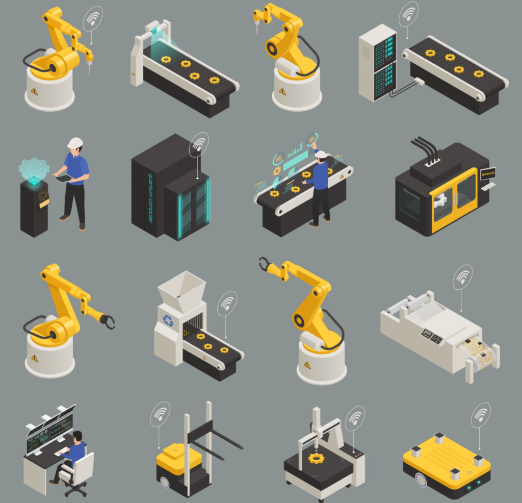
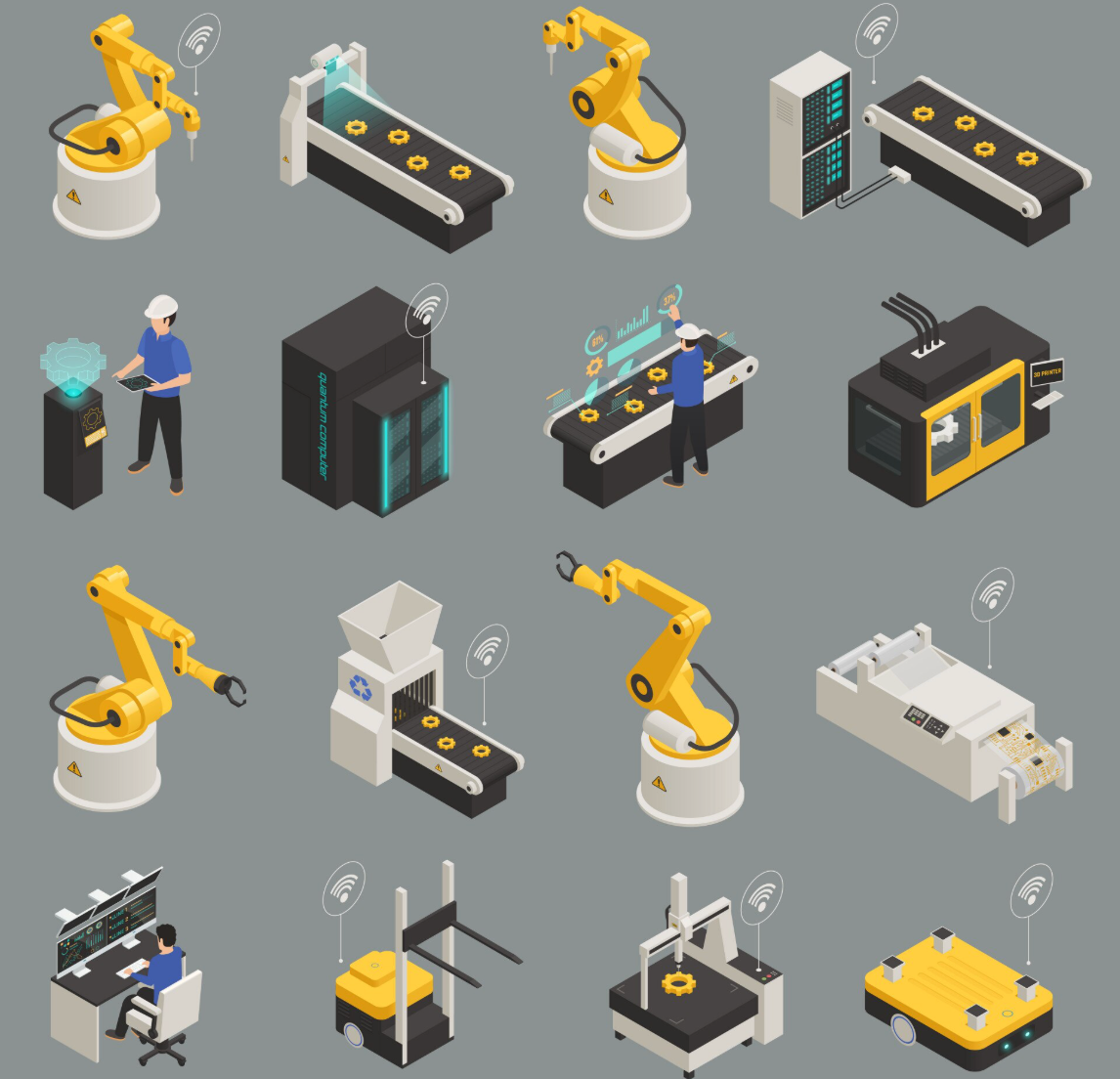
Smart manufacturing automation is revolutionizing PCBA production. AI-driven predictive maintenance prevents unexpected breakdowns by scheduling maintenance during non-disruptive times. This approach reduces emergency repairs and minimizes costly downtime. Real-time equipment status monitoring via sensors provides data for intelligent abnormality warnings, alerting engineers to potential faults. This allows maintenance during planned breaks, preventing quality impacts. This results in greatly reduced unplanned downtime and stable production. Predictive maintenance can reduce equipment-related defects by 50% and unplanned downtime by 80%.
Robotic handling systems further enhance efficiency and precision in PCBA assembly. Robotics improves PCB assembly through high-speed pick-and-place operations, achieving sub-millimeter accuracy for fine-pitch components. This boosts throughput and consistency. AI robot PCB assembly is essential when edge computing and high-speed memory routing demand HDI-level precision. These robots work tirelessly, improving the speed and efficiency of the assembly process. The smart manufacturing ecosystem integrates AI vision inspection, deep learning models, and predictive defect prevention. It also includes digital twins, which are virtual factory models that simulate production processes to identify risks. This intelligent automation, combined with data-driven decision making and human-machine collaboration, creates a highly efficient and sustainable manufacturing environment. Connectivity via IIoT provides end-to-end visibility of material flow and machine status. This comprehensive approach to smart manufacturing reduces rework, shortens handoff times, and minimizes documentation overhead, ultimately accelerating time-to-market for AI hardware products. This commitment to green manufacturing principles also supports sustainability goals.
Partnering with US-based pcba assembly providers offers significant advantages for AI hardware startups. These benefits include rapid prototyping, robust supply chain security, and adherence to stringent quality standards. Domestic manufacturing proves crucial for fostering innovation, ensuring intellectual property protection, and accelerating time-to-market in the AI hardware sector. The synergy between advanced pcba services and the growing AI industry in the USA will continue to drive technological progress. AI hardware startups should seek electronics manufacturing partners who deeply understand their unique needs, supporting their journey from initial concept through successful market launch with high-quality pcba.
FAQ
What specific PCBA challenges do AI hardware startups face?
AI hardware startups often encounter rapid prototype iteration needs and complex designs. They deal with intricate BGA and high-speed interfaces. Many also lack cooperative manufacturing teams. These factors demand specialized expertise in pcb assembly and efficient production processes.
How do US-based PCBA services support rapid innovation for startups?
US-based services offer one-stop delivery from Gerber files and BOMs to prototyping, small-batch production, and functional testing. They provide rapid PCB prototyping, efficient BOM procurement, SMT, X-Ray, and functional testing. This accelerates design cycles and ensures quality for AI hardware.
Why is domestic PCBA manufacturing important for AI hardware?
Domestic manufacturing provides a resilient supply chain and robust intellectual property protection. It ensures compliance with strict regulatory standards like ITAR and EAR. This approach minimizes delays and secures sensitive data, which is crucial for advanced AI hardware development and assembly.
What documentation do I need for a PCBA quotation?
For a pcb assembly quotation, you typically need a Bill of Materials (BOM), Gerber files, and a Centroid file. These documents provide essential data for the manufacturer. They allow accurate assessment of project requirements and precise cost estimation for your PCB project.
See Also
Tailored Edge Artificial Intelligence Circuit Boards For American Tech Startups
Bespoke Artificial Intelligence Circuit Board Production For Mexican Electronics Firms
Complete Artificial Intelligence Hardware Assembly For Irish Medical And Smart Devices
Specialized Artificial Intelligence Server Prototype Assembly For Israeli Infrastructure Innovators
Smart Internet Of Things Circuit Board Manufacturing For Malaysian Hardware Enterprises