
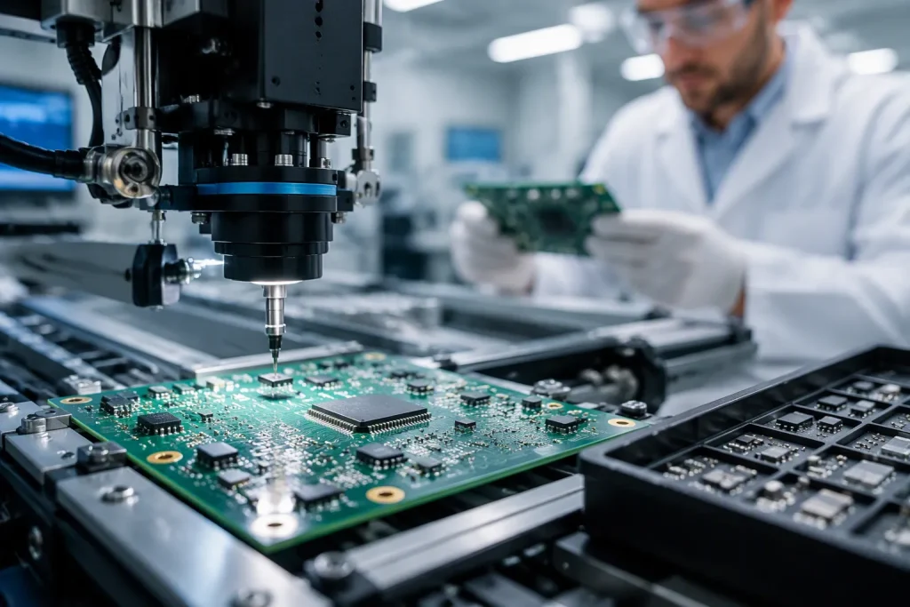
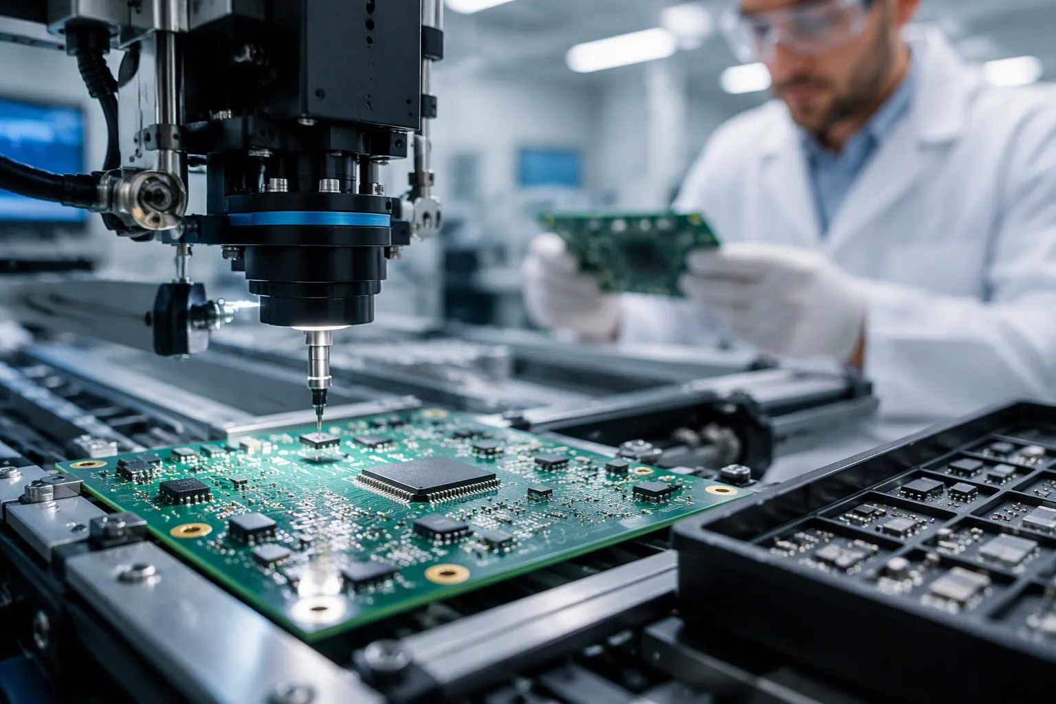
Edge AI PCBA assembly is the manufacturing process that builds printed circuit board assemblies capable of running artificial intelligence inference locally on the device. This work sits at the center of modern ai hardware pcb assembly, where processors, memory, and sensors must cooperate inside tight enclosures.
Processing has moved from cloud servers toward edge devices. Cameras, inference boxes, smart terminals, and gateways now execute models on site. Latency drops, private data stays local, and bandwidth costs fall.
Performance, power, thermals, and reliability all converge on one board. Each decision shapes the final product. Skilled ai hardware pcb assembly partners treat these demands as one system, not separate tasks.
Key Takeaways
Edge AI PCBA assembly builds boards that run AI locally, cutting latency and keeping data private.
Design boards with power sequencing, impedance control, and fanless cooling for reliable performance.
Use advanced processes like HDI and via-in-pad to handle fine-pitch components and dense interconnects.
Test power, interfaces, and inference workloads to ensure each board meets quality standards.
Choose a partner with certifications and experience to scale from prototype to mass production.
What Is Edge AI PCBA Assembly?
PCBA Defined for Edge AI
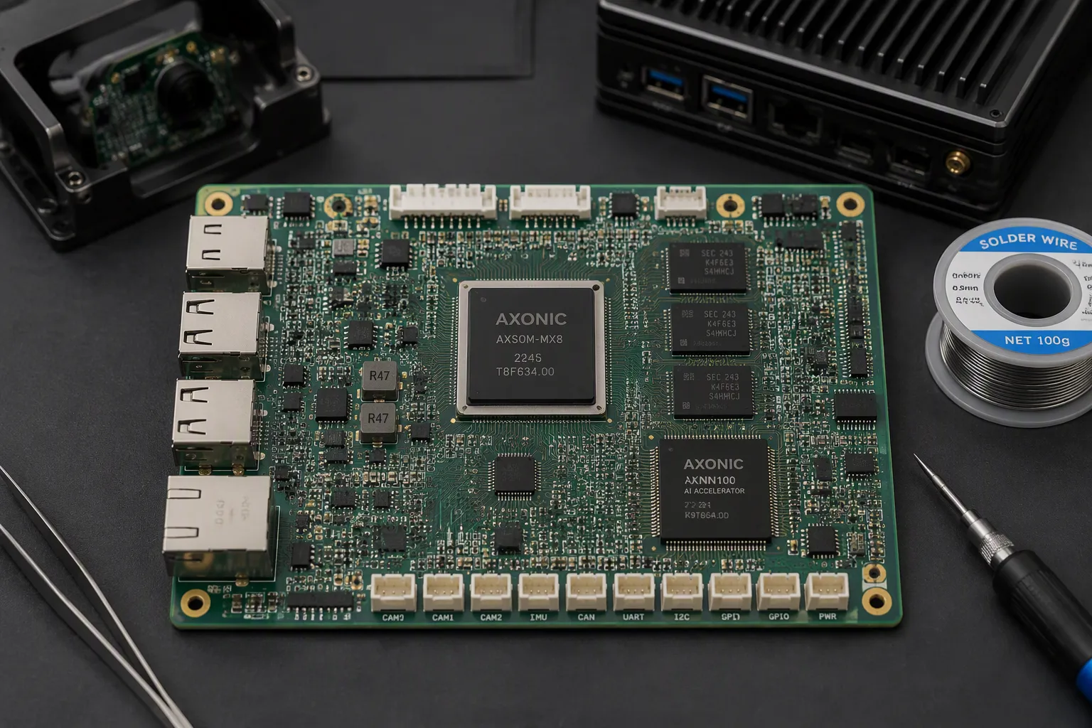
Edge AI PCBA assembly is the manufacturing process for printed circuit board assemblies that run AI inference locally on the device. The board itself becomes the compute platform. A processor, memory, storage, and sensor interfaces all sit on one substrate, and the model executes there instead of in a remote data center.
This definition separates edge AI work from conventional electronics production. A standard control board moves signals and switches loads. An inference board must sustain continuous matrix computation, feed a neural accelerator with data, and hold thermal and power behavior inside a fixed envelope. The distinction shapes every downstream choice, from stackup to solder joint inspection.
Representative products built this way include AI cameras, edge inference boxes, smart terminals, and AI gateways. Each one ships intelligence inside the enclosure. A camera classifies what it sees. A gateway filters and routes model output. An inference box serves a small cluster of local devices. The common thread is local decision-making with no round trip to a server.
Why AI Is Moving to the Edge
Four forces drive the shift away from centralized inference. Latency comes first. Factory automation and medical monitoring treat milliseconds as non-negotiable, and a cloud round trip adds delay the application cannot absorb. Robotics must decide within milliseconds, and 5G URLLC exists precisely to enable millisecond-level response times. Autonomous vehicles, industrial automation, and patient monitoring all fall into the same category. A security camera detects intruders and triggers alarms without waiting for a cloud response, which shortens reaction time and removes a dependency on network availability.
Privacy follows. Video and biometric data stay on the device, which simplifies compliance and reduces exposure. Bandwidth is the third driver. Streaming raw sensor data to a remote server consumes capacity that many deployments cannot justify. Cost closes the loop. Cloud inference charges scale with usage, and a fixed local processor spreads that expense across the product lifetime.
The comparison below frames the tradeoff that buyers weigh during specification.
Factor | Cloud inference | On-device inference |
|---|---|---|
Response time | Network round trip added | Local, immediate |
Data exposure | Payload leaves the device | Data stays on board |
Bandwidth use | Continuous upstream stream | Minimal |
Cost model | Usage-based, recurring | Fixed at build |
Two pain points dominate customer conversations. Cloud inference latency limits what a product can promise, and power plus thermal control inside a sealed enclosure constrains how much compute fits. High-density, low-power PCBA design answers both. Dense interconnect shortens signal paths, and efficient power delivery keeps heat manageable. These constraints define the requirements covered next.
Core On-Device AI PCB Requirements
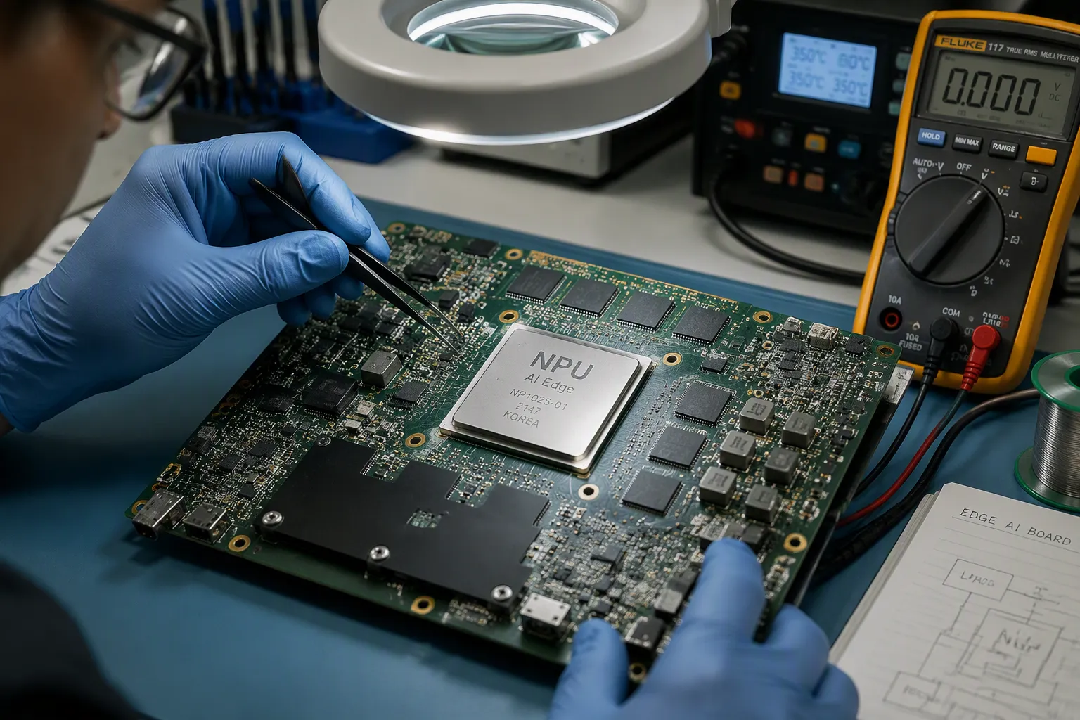
The foundation of edge ai pcba assembly rests on electrical integrity, thermal control, and mechanical durability. The board must deliver clean power to high-speed processors, maintain signal integrity across dense interconnects, and shed heat without active cooling.
Electrical Performance and Mixed-Signal Integrity
Power sequencing is the first concern for ai hardware pcb assembly. An NPU, memory controller, and storage interface each require specific voltage rails that ramp up in a defined order. A timing violation can latch the system or cause latent failures. SoC and memory control demand tight impedance matching. High-speed memory interfaces such as GDDR6 or LPDDR operate in the GHz range. Any mismatch in trace impedance, via structure, or reference plane continuity degrades the signal. Storage imaging adds further precision requirements for the pcb assembly.
Several signal integrity challenges arise on boards that require ai hardware pcb assembly. High pin density in large BGA or LGA packages forces dense breakout routing with limited space. Narrow traces and multiple layer transitions create impedance discontinuities at each via. Thick multilayer structures introduce longer vias with stub effects that cause reflections and resonances with fast-rise-time signals. Socket interfaces and connectors add insertion loss, parasitic inductance, and return-path disruption. Power integrity also affects signal integrity. Dynamic PDN behavior under high-speed switching causes voltage droop, ground bounce, and simultaneous switching noise. Decoupling challenges arise because mechanical constraints push capacitors farther from the DUT, adding inductance and raising PDN impedance.
Attenuation becomes critical at GHz frequencies. Low-loss substrate materials such as Panasonic Megtron or Rogers Tachyon series reduce dielectric and conductor losses for AI memory interfaces. Reflection and impedance mismatch demand strict ±5% tolerance control across trace width and dielectric thickness. Crosstalk between parallel high-speed traces requires the 3W spacing rule and ground planes between critical networks. Layer transitions must be minimized and backdrilling used to remove via stubs. Reference plane continuity must be maintained across all critical signal layers. Simulation-driven design anticipates all these issues during the layout phase. The entire pcb assembly must account for these factors during the pcb assembly process.
Thermal Management and NPU/SoC Power Design
Edge AI devices rarely include fans. The enclosure seals against dust and moisture. Heat must move through the board to a chassis or heatsink. Power delivery to the NPU and SoC creates concentrated hot spots. In fanless designs, thermal dissipation becomes the primary limiter of sustained performance in any ai hardware pcb assembly.
Thermal throttling is the most common consequence for ai hardware pcb assembly. Processors reduce clock speed automatically when junction temperature exceeds a threshold, lowering inference throughput. System instability follows when heat affects voltage regulation and timing, causing crashes or unexpected reboots. Consistent high temperatures accelerate silicon aging and can cause solder fatigue, particularly affecting NAND flash memory. High temperatures reduce mean time between failures for capacitors and integrated circuits. Emergency thermal protection can trigger unexpected shutdowns, causing operational downtime. Accuracy loss occurs when heat-related slowdowns introduce delays and reduce inference reliability, leading to missed detections or jittery sensor readings.
The table below summarizes the relationships between thermal stress and operational impact.
Thermal issue | Operational effect |
|---|---|
Thermal throttling | Reduced inference throughput |
System instability | Crashes or reboots |
Component wear | Lower MTBF, data corruption risk |
Accuracy loss | Missed detections, sensor jitter |
Emergency shutdown | Operational downtime |
Mechanical robustness matters for edge deployments. Vibration, shock, and temperature cycling are common in factory or outdoor environments. The PCBA must withstand these conditions without solder joint fatigue. IPC-A-610 Class 2 or Class 3 acceptance criteria apply to solder joints and component placement. Advanced ai processing boards use rigid-flex construction and reinforced mounting points. Manufacturing these boards requires precise control of pcb material selection and stackup. Each pcb assembly must pass rigorous quality checks. The hardware design must also consider thermal interface materials and mounting torque specifications.
Specialized Edge AI Assembly Processes
High-Density and Advanced Packaging
Fine-pitch BGA devices demand via-in-pad technology for signal breakout. Reliable assembly requires resin filling, copper plating, and planarization. Poorly filled vias cause solder voids or open joints during reflow. Laser drilling creates microvias as small as 20 μm with ±5 μm accuracy. Sequential lamination prevents layer shifting and ensures precise alignment.
The table below maps package pitch to required PCB structure.
Component | Ball/Pad Pitch | Required PCB Structure |
|---|---|---|
BGA | 0.65 mm | HDI 1+N+1 |
BGA | 0.4 mm | HDI 2+N+2 or any-layer |
CSP/WLCSP | ≤ 0.3 mm | Any-layer HDI |
System-in-package substrates function like HDI PCBs, providing high-density interconnect between chips. This approach improves signal speed, reduces parasitic effects, and saves size and weight. Bonysn supports these advanced ai hardware pcb assembly requirements through HDI and multilayer capabilities.
AI Robot PCB Assembly Reliability
Robotic PCB manufacturing and assembly services conform to IPC Class 3 standards. This level is required for handling fine-pitch components like LCC, BGA, and QFN in modern automation hardware.
Robotic PCB manufacturing and assembly services fully conform to IPC Class 3 industry standards, and support ISO9001 quality management, ISO13485 traceability management, and other certifications.
Testing follows IPC TM-650 for impedance measurement and IPC-9252B for continuity and isolation. ANSI/ESD S20.20 governs ESD protection. For ai robot pcb assembly, precise testing and stable PCBA solutions ensure reliability. Bonysn coordinates thermal solutions and functional testing to support ai robot sensor module pcb production. The ai hardware pcb assembly process for ai robotics pcb manufacturing demands precision and consistency across every board.
Prototyping, DFM, and PCBA Testing
Design-for-Manufacturing for Smooth Scaling
Prototyping edge AI hardware demands assembly techniques that translate directly to volume production. Double-sided assembly places components on both surfaces, which increases routing density and shortens critical signal paths. Rigid-flex construction bends the board into compact shapes without connectors, improving reliability in vibration-prone deployments. Both approaches require careful panelization and stencil design from the first prototype.
Design-for-manufacturing reviews catch problems before tooling commitments. Engineers examine pad geometry, component spacing, and thermal relief patterns. They verify that fine-pitch devices have adequate solder paste volume and that via-in-pad structures will fill correctly. These steps reduce rework and accelerate the transition to mass production. A disciplined DFM process also protects consistency across production lots.
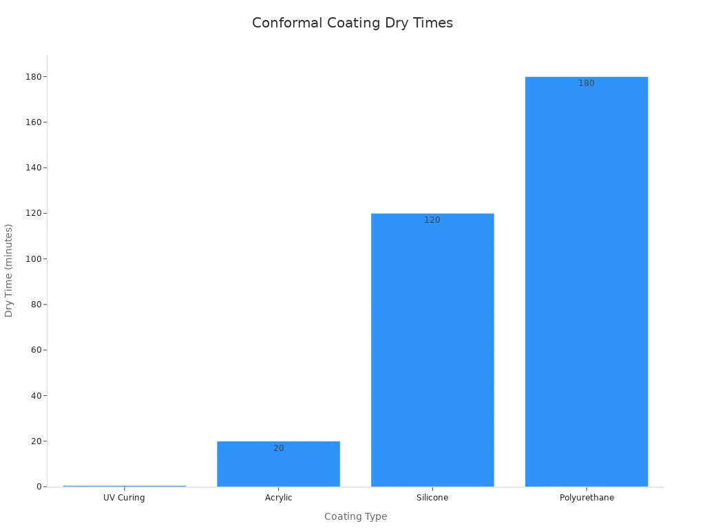
Conformal coating extends protection to outdoor edge AI deployments. The process follows five steps: thorough cleaning, masking sensitive areas, controlled application, proper curing, and quality testing. Coating type affects repairability and thermal performance. IPC-CC-830B governs material qualification, while IPC-A-610 provides workmanship criteria.
PCBA Testing Priorities for Edge AI
Testing validates every pcba before shipment. Power sequencing tests confirm that voltage rails ramp in the correct order. Interface testing exercises memory buses, storage controllers, and sensor connections under load. Functional validation runs actual inference workloads to verify throughput and thermal behavior.
For ai robot sensor module pcb production, testing must confirm signal integrity across vibration profiles. Scalable robotics production depends on repeatable test fixtures and documented pass criteria. Each pcb assembly undergoes impedance measurement per IPC TM-650 and continuity checks per IPC-9252B. These steps ensure that ai hardware pcb assembly meets reliability targets.
Choosing an Edge AI PCBA Assembly Partner
Capabilities and Certifications to Check
Component sourcing, testing, and box build services form the backbone of a reliable supply chain. A strong partner manages procurement, verifies incoming parts, and delivers a finished unit ready for deployment. These services reduce coordination overhead and protect quality at every stage.
Certifications separate qualified suppliers from the rest. Automotive AI hardware may require IATF 16949 compliance.
IATF 16949 certification is merely the entry ticket; manufacturers must also complete a series of systematic certifications such as PPAP, APQP, and FMEA, while meeting product lifecycle and supply guarantee requirements of over 10 years.
For safety-critical programs, ISO 26262 ASIL-D represents the highest functional safety level. AEC-Q qualification, wide temperature tolerance from –40°C to +125°C, and strong EMI shielding round out the automotive-grade checklist.
The table below maps key IPC standards to their role in edge AI work.
IPC Standard | Relevance to Edge AI PCBA Assembly |
|---|---|
IPC-A-600 | Bare board acceptability criteria |
IPC-A-610 | Assembly soldering and placement quality |
IPC-2221 | Design guidelines for traces and stackups |
IPC-J-STD-001 | Soldering requirements for assemblies |
Bonysn supports HDI, multilayer PCB, and BGA assembly for demanding edge designs. Their thermal solutions and functional testing capabilities serve ai robotics pcb manufacturing programs that require stable output.
Questions to Ask Before Committing
A short evaluation checklist sharpens the selection process. Ask about component sourcing policies, traceability systems, and test coverage. Confirm the partner holds relevant certifications and can provide documentation packages. Inquire about capacity for mass production and experience with fine-pitch devices.
US-based AI hardware PCB manufacturers offer speed, quality, and innovation advantages. Local production shortens lead times and simplifies communication. Bonysn coordinates thermal solutions and functional testing to support ai robot sensor module pcb production. Their ai hardware pcb assembly process covers prototyping through volume, and their electronics manufacturing team handles complex ai hardware pcb assembly requirements. For any ai hardware pcb assembly project, verify that the partner can scale without sacrificing consistency.
Edge AI PCBA assembly succeeds when electrical, thermal, mechanical, and testing demands are treated as one system. Power sequencing, impedance control, and fanless heat dissipation decide whether a design meets its targets. Early DFM involvement cuts rework during scaling. The right partner brings pcb assembly and pcba testing to every program.
Edge AI hardware will keep evolving. Embedded computing, AI-optimized silicon, and signal integrity above 25 Gbps push board design toward finer features. Every ai hardware pcb assembly partner must adapt manufacturing lines.
Begin with a DFM review. Bonysn supports ai hardware pcb assembly from prototype through volume. Their electronics manufacturing team validates each pcba. Choose an ai hardware pcb assembly partner.
FAQ
How does edge AI PCBA assembly differ from standard PCBA manufacturing?
Edge AI boards run inference locally. They need power sequencing for NPUs, impedance control for high-speed memory, and fanless thermal design. Standard boards move signals. AI boards sustain matrix computation. This shapes stackup, materials, and testing. Market demand for local inference drives this shift.
What thermal challenges affect on-device AI hardware?
Fanless enclosures trap heat. Throttling cuts inference throughput. High temperatures lower MTBF and risk solder fatigue. Designers use thermal vias, metal cores, and rigid-flex to move heat. IPC-A-610 Class 2 or 3 governs joint quality. These pain points define edge deployments.
Which tests validate an edge AI PCBA before shipment?
Power sequencing tests confirm rail order. Interface tests exercise memory and sensors under load. Functional validation runs real inference workloads. Impedance measurement follows IPC TM-650. Continuity checks follow IPC-9252B. These steps ensure reliable pcb assembly. Bonysn performs these tests for every board.
How does Bonysn support robot PCB assembly reliability?
Bonysn conforms to IPC Class 3 for robot fine-pitch components. They support ISO9001 and ISO13485 traceability. Their thermal solutions and functional testing serve ai robot sensor module pcb production. They coordinate prototyping through volume for stable output. This approach meets market demand for reliable robot hardware.
What should buyers ask an edge AI PCBA partner?
Ask about component sourcing, traceability, and test coverage. Confirm certifications like IATF 16949 for automotive work. Inquire about capacity for mass production and fine-pitch experience. US-based manufacturers offer speed and quality advantages. Bonysn supports HDI, multilayer pcb, and BGA assembly for demanding edge designs.
See Also
Exploring Openai Hardware Trends Impact On Custom Ai Pcba
Designing Pcb Assembly For Openai Inspired Ai Companion Device
Bespoke Edge Ai Pcba For United States Hardware Startups
Pcb Assembly For Edge Ai In Canadian Vision Monitoring Devices